Method of manufacturing gallium nitride substrate and gallium nitride substrate manufactured by the same

A technology of gallium nitride substrate and gallium nitride film, which is applied in the field of manufacturing gallium nitride substrate and gallium nitride substrate manufactured by the same, can solve the problem of difficult to control GaN film, achieve improved characteristics and productivity, and improve process Efficiency, crack reduction effect

Inactive Publication Date: 2014-01-22
SAMSUNG CORNING PRECISION MATERIALS CO LTD
View PDF10 Cites 3 Cited by
  • Summary
  • Abstract
  • Description
  • Claims
  • Application Information

AI Technical Summary

Problems solved by technology

However, when the low-quality GaN film is removed, the thickness of the remaining high-quality GaN film becomes 200 μm or less, and it is difficult to handle the GaN film, which becomes a problem

Method used


Image

  • Method of manufacturing gallium nitride substrate and gallium nitride substrate manufactured by the same
  • Method of manufacturing gallium nitride substrate and gallium nitride substrate manufactured by the same
  • Method of manufacturing gallium nitride substrate and gallium nitride substrate manufactured by the same

Examples


Embodiment Construction

[0053] Reference will now be made in detail to a method of manufacturing a gallium nitride (GaN) substrate and a GaN substrate manufactured by the method according to the present invention, the embodiments of which are illustrated in the accompanying drawings and described below so that those of ordinary skill in the art to which the present invention pertains can understand The invention is easily put into practice.

[0054] Throughout, reference should be made to the drawings, wherein the same reference numerals and symbols are used throughout the different drawings to indicate the same or similar parts. In the following description of the present invention, a detailed description of known functions and components incorporated herein will be omitted when it would make the subject matter of the present invention unclear.

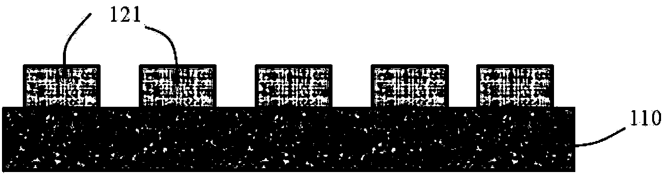
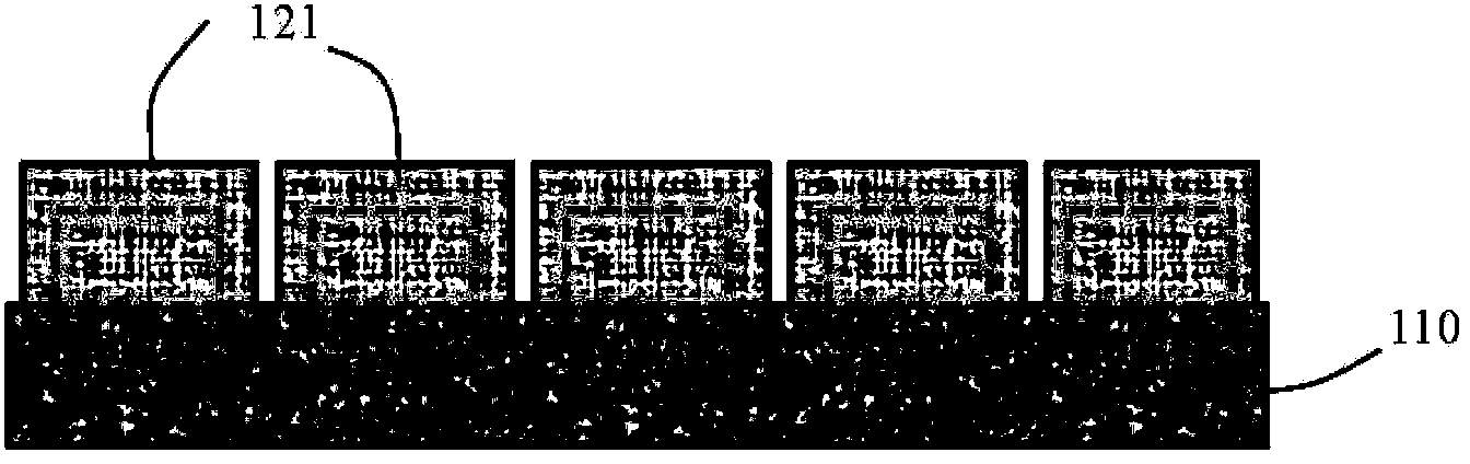
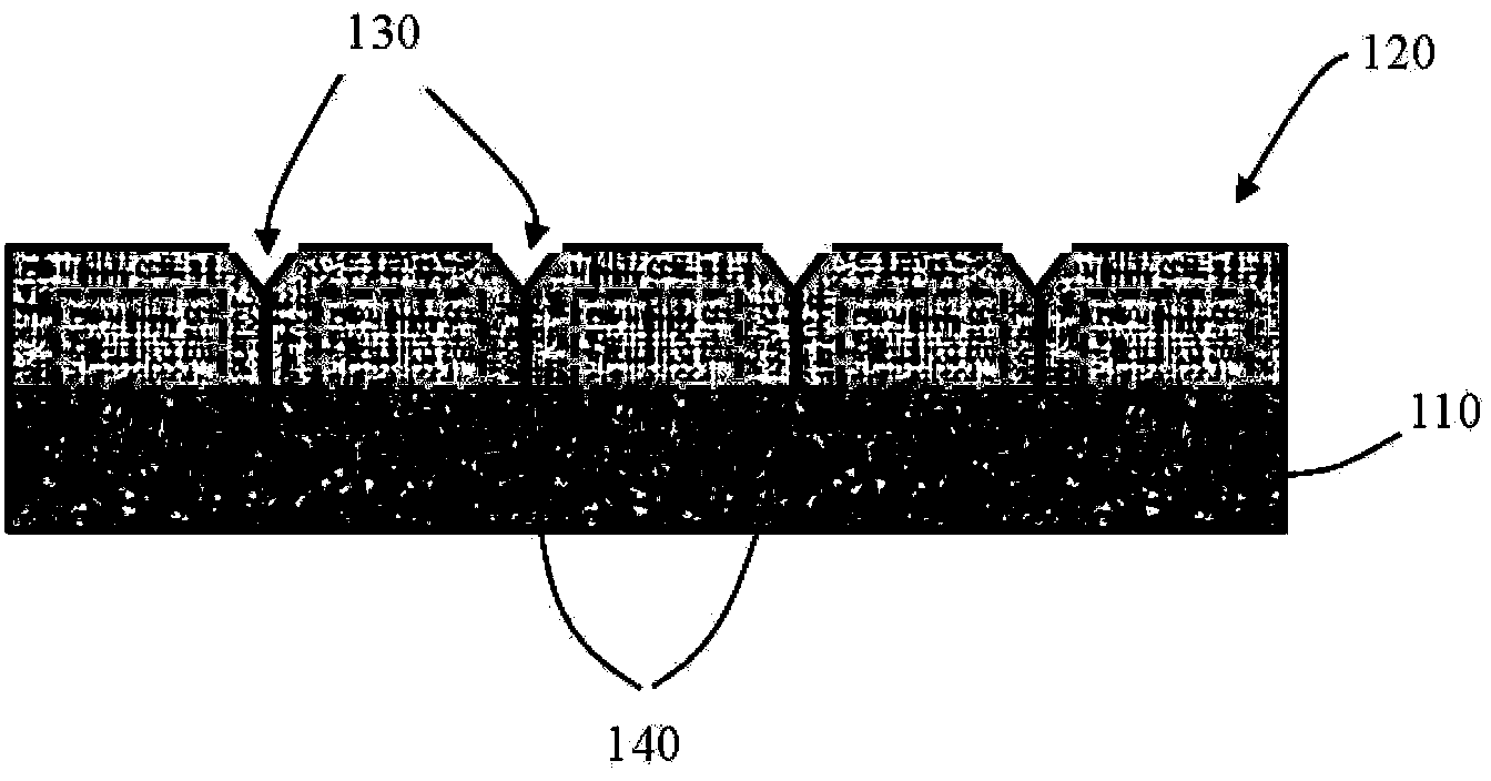
[0055] A method of manufacturing a GaN substrate according to an embodiment of the present invention is to manufacture a free-standing GaN substrate ( Fi...


PUM

PropertyMeasurementUnit
temperatureaaaaaaaaaa
thicknessaaaaaaaaaa

Abstract

A method of manufacturing a gallium nitride (GaN) substrate and a GaN substrate manufactured by the same. The method includes the steps of growing a GaN film on a base substrate and separating the base substrate from the GaN film. The step of growing the GaN film includes forming pits in the GaN film, the pits inducing an inversion domain boundary to be formed inside the GaN film. The GaN substrate can have a predetermined thickness with which it can be handled during layer transfer (LT) processing, and the warping of the GaN substrate can be minimized, thereby preventing cracks due to warping.

Description

[0001] Cross References to Related Applications [0002] This application claims priority to Korean Patent Applications Nos. 10-2012-0070389 and 10-2012-0147987 filed on June 29, 2012 and December 18, 2012, the entire contents of which are in all respects The statement is incorporated herein by reference. technical field [0003] The present invention relates to a method of manufacturing a gallium nitride (GaN) substrate and a gallium nitride substrate manufactured by the method, and more particularly, to a method of manufacturing a GaN substrate and a GaN substrate manufactured by the method, wherein the GaN substrate may have The layer transfer (LT) process can be used to manipulate the predetermined thickness of the substrate, and the warpage of the GaN substrate can be minimized, thereby preventing cracks due to warpage. Background technique [0004] Gallium nitride (GaN) is a direct-transition semiconductor material with a bandgap energy of 3.39eV, and can be used to m...

Claims


Application Information

Patent Timeline
Patent Type & Authority Applications(China)
IPC IPC(8): C30B29/40C30B23/02C30B25/02H01L21/02
CPCH01L33/0075H01L21/02502H01L21/02458H01L21/02513H01L21/0262C30B29/406H01L21/02664C30B25/16C30B25/02H01L21/0237H01L21/0254
Inventor 林圣根朴甫益禹广济金宇理汉金俊会朴喆民裵峻莹李东龙李原兆崔准成
Owner SAMSUNG CORNING PRECISION MATERIALS CO LTD
Why Eureka
Try Eureka