Transmission electron microscope sample table of in-situ measurement nanometer device

A technology of transmission electron microscope samples and nano-devices, which is applied in the direction of measuring devices, instruments, circuits, etc., can solve the problems of narrow space for placing samples, difficulty in measuring electrical signals, and difficulty in installing multi-electrodes, etc., to achieve reliable performance, expanded functions, The effect of easy installation

Inactive Publication Date: 2014-01-22
SOUTHEAST UNIV
View PDF4 Cites 9 Cited by
  • Summary
  • Abstract
  • Description
  • Claims
  • Application Information

AI Technical Summary

Problems solved by technology

Existing technology cannot meet the measurement of multi-electrode nanodevices
Transmission electron microscopy is a powerful tool for studying the structure and properties of nanomaterials because it can observe samples at atomic-scale resolution. However, the space for placing samples between the pole pieces of the objective lens in transmission electron microscopy is very narrow, especially for sub-nanometer-scale resolution. The c

Method used


Image

  • Transmission electron microscope sample table of in-situ measurement nanometer device
  • Transmission electron microscope sample table of in-situ measurement nanometer device
  • Transmission electron microscope sample table of in-situ measurement nanometer device

Examples


Embodiment Construction

[0021] Below in conjunction with accompanying drawing and specific embodiment, further illustrate the present invention, should be understood that these embodiments are only for illustrating the present invention and are not intended to limit the scope of the present invention, after having read the present invention, those skilled in the art will understand various aspects of the present invention Modifications in equivalent forms all fall within the scope defined by the appended claims of this application.

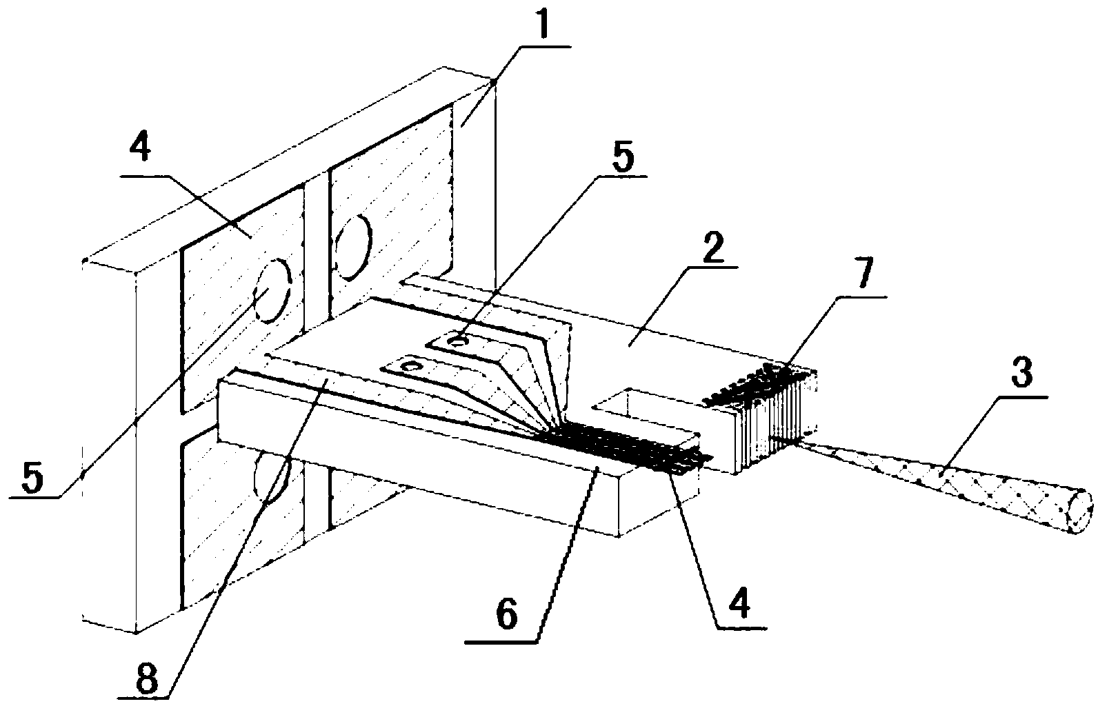
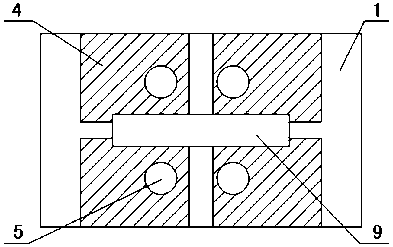
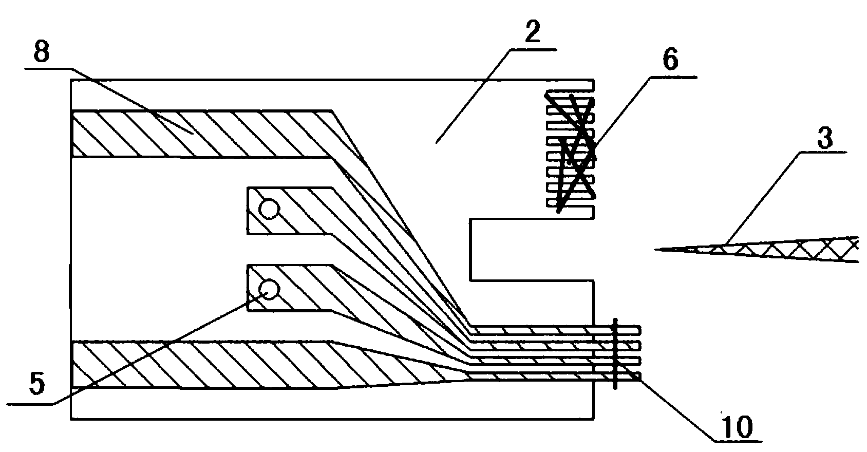
[0022] Such as figure 1 As shown, a transmission electron microscope sample stage for in-situ measurement of the electrical properties and atomic structure of graphene field effect transistors, including an insulating block, a sample support table and a metal nanoprobe, and four metal Electrodes, and the metal electrodes on the front and back sides are electrically connected through metallized through holes; at the same time, the insulating block is provided with a slot ...


PUM


Abstract

The invention discloses a transmission electron microscope sample table of an in-situ measurement nanometer device. The transmission electron microscope sample table comprises a metal nanoprobe, an insulating plug piece and a sample supporting table, wherein the front and reverse surfaces of the insulating plug piece are provided with a plurality of metal electrodes respectively; the corresponding metal electrodes are conductively connected through metallized through holes; one end of the sample supporting table is connected with the insulating plug piece, and the other end of the sample supporting table is provided with a sampling region and a testing region; the testing region is a metal electrode which is arranged on the surface of the sample supporting table and is suspending; the metal electrode of the sample supporting table is conductively connected with the metal electrode of the insulating plug piece; the metal nanoprobe, the testing region metal electrode and a tested sample form a three-end field effect transistor. According to the transmission electron microscope sample table, the sample can be observed under the atomic-scale resolution and electrical measurement is performed in real time, and the electrical property and the nanostructure change of a unit to be measured are disclosed in situ.

Description

[0001] technical field [0002] The invention belongs to the field of in-situ measurement of nano-device performance, and in particular relates to a multi-electrode transmission electron microscope sample stage for in-situ measurement of the electrical properties and atomic structure of graphene field effect tubes. A multi-electrode device construction area and a nanomaterial sampling area are prepared on the sample. Background technique [0003] In the field of nanoelectronic devices, graphene two-dimensional materials are considered to be the successor of silicon. Graphene is a monoatomic layer planar film composed of carbon atoms, which has the characteristics of high conductivity, high strength, and ultra-thin. To study the electrical response and physical morphology changes of graphene-based field-effect transistors under an applied electric field state, and to collect data on their electrical characteristics is the basic goal of current design and development of graph...

Claims


Application Information

Patent Timeline
IPC IPC(8): H01J37/20G01N23/00
Inventor 吴幸孙立涛余开浩吴旻骏潘弘扬邢雪马子哲
Owner SOUTHEAST UNIV
Why Eureka
Try Eureka