Manufacturing method for semiconductor device

A device manufacturing method and semiconductor technology, applied in semiconductor/solid-state device manufacturing, semiconductor devices, electrical components, etc., can solve problems such as substrate damage, achieve the effects of improving gate control capabilities, reducing EoT, and optimizing threshold voltage

Active Publication Date: 2014-01-22
INST OF MICROELECTRONICS CHINESE ACAD OF SCI
View PDF9 Cites 2 Cited by
  • Summary
  • Abstract
  • Description
  • Claims
  • Application Information

AI Technical Summary

Problems solved by technology

In particular, the current sidewall etching technology is generally based on Ar-based gas, which is easy to cause damage to the substrate under the condition of nanoscale devices

Method used


Image

  • Manufacturing method for semiconductor device
  • Manufacturing method for semiconductor device
  • Manufacturing method for semiconductor device

Examples


Embodiment Construction

[0026] The features and technical effects of the technical solution of the present invention will be described in detail below with reference to the accompanying drawings and in combination with exemplary embodiments. It should be pointed out that similar reference numerals represent similar structures, and the terms "first", "second", "upper", "lower", "thick", "thin" and the like used in this application can be used for Modify various device structures. These modifications do not imply a spatial, sequential or hierarchical relationship of the modified device structures unless specifically stated.

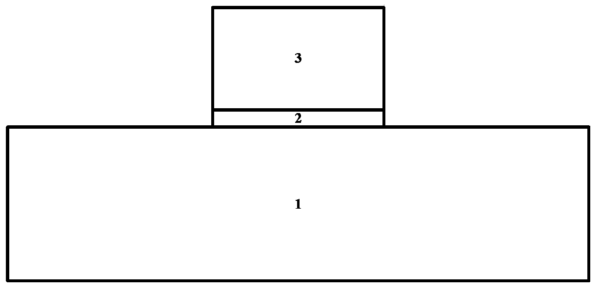
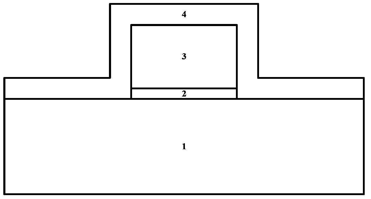
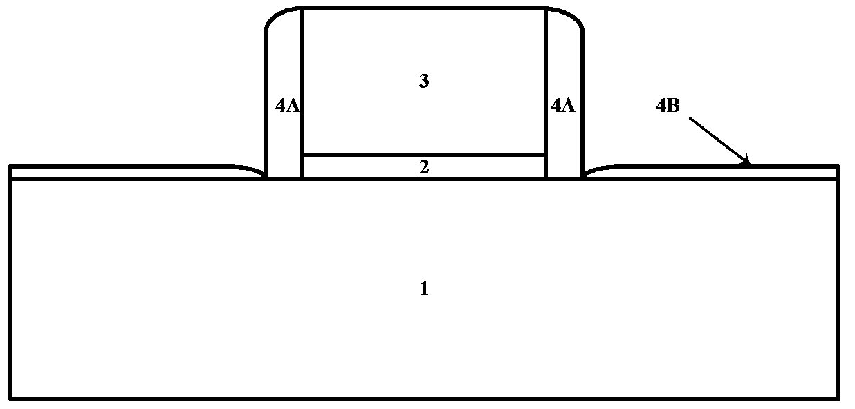
[0027] refer to Figure 5 as well as figure 1 , forming a gate stack structure on the substrate, which may be a gate stack structure of a gate-first process, or a dummy gate stack structure of a gate-last process. A substrate 1 is provided, which can be bulk Si, SOI, bulk Ge, GeOI, Si Ge, GeSb, or a III-V or II-VI compound semiconductor substrate, such as GaAs, GaN, InP, InSb,...


PUM

PropertyMeasurementUnit
thicknessaaaaaaaaaa

Abstract

Provided is a manufacturing method for a semiconductor device. The method comprises: forming a stacked gate structure on a substrate; depositing a dielectric material layer on the substrate and the stacked gate structure; performing main etching to etch the dielectric material layer to form a side wall, and leaving residues of the dielectric material layer on the substrate; and performing over-etching to remove the residues of the dielectric material layer. According to the provided manufacturing method for the semiconductor device, instead of using a silicon oxide etching barrier layer, a two-step etching by using an etching gas containing helium is performed so that while the damage to the substrate is reduced, the process complexity is also reduced, and besides, the threshold voltage can be optimized, the EoT can be effectively reduced, and the gate-control capability and the drive current can be increased.

Description

technical field [0001] The invention relates to the field of semiconductor integrated circuit manufacturing, and more specifically, to a sidewall etching method. Background technique [0002] In VLSI manufacturing, dielectric spacers need to be made before the lightly doped drain (LDD) implantation process to prevent source-drain implantation of a larger dose from being too close to the channel to cause source-drain breakthrough, resulting in device failure and reduced yield. [0003] The current mainstream 65nm or even 45nm sidewall manufacturing process is: before the lightly doped drain (LDD) implantation process, first deposit or thermally grow a layer of silicon dioxide film, such as rapid thermal oxidation (RTO) growth Silicon dioxide on the left and right is used as a subsequent etching barrier to protect the substrate, especially the interface between the source and drain regions close to the channel region, from damage, so as to avoid the increase of defect densit...

Claims


Application Information

Patent Timeline
Patent Type & Authority Applications(China)
IPC IPC(8): H01L21/3065H01L21/28
CPCH01L21/28008H01L29/66545H01L21/28017
Inventor 孟令款
Owner INST OF MICROELECTRONICS CHINESE ACAD OF SCI
Why Eureka
Try Eureka