

Piezoelectric electret material and preparation method thereof
A piezoelectric electret, electret technology, applied in the material selection of piezoelectric devices or electrostrictive devices, the manufacture/assembly of piezoelectric/electrostrictive devices, the selection of device materials, etc., can solve the problem of Limited charge storage, etc.
- Summary
- Abstract
- Description
- Claims
- Application Information
AI Technical Summary
Problems solved by technology
Method used
Image

Examples
preparation example Construction
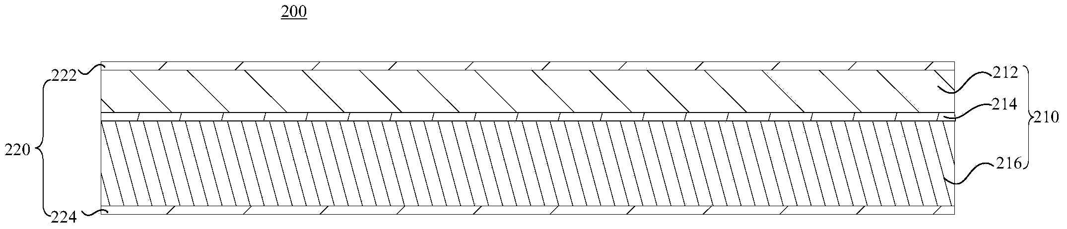
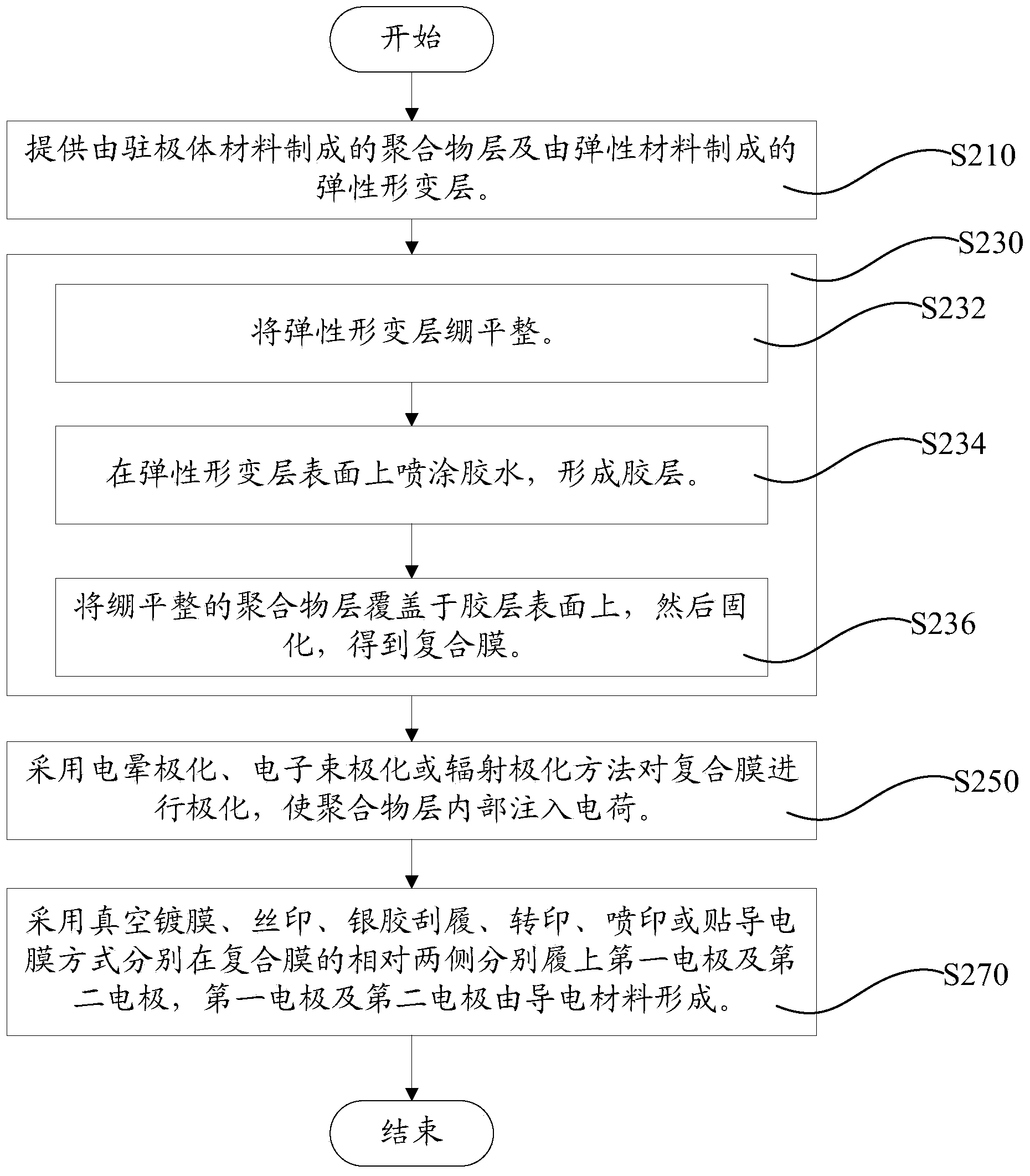
[0046] see image 3 , the preparation method steps of the piezoelectric electret material 200 in the above-mentioned first embodiment include the following steps:
[0047] Step S210 , providing the polymer layer 212 made of electret material and the elastic deformation layer 216 made of elastic material, wherein the elastic modulus of the elastic material is in the range of 0 MPa˜100 MPa.
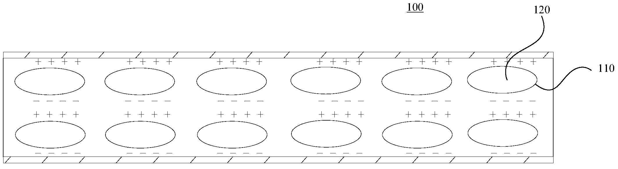
[0048] The electret material can be selected from polytetrafluoroethylene (Polytetrafluoroethene, PTFE), fluorinated ethylene propylene copolymer (Fluorinated ethylene propylene, FEP), polypropylene (Polypropylene, PP), perfluoroalkoxy resin (Polyfluoroalkoxy, PFA ), polychlorotrifluoroethylene (PCTFE), polyvinylidene fluoride (PVDF) or polyethylene naphthalate (polyethylene naphthalate, PEN). The thickness of the polymer layer 212 may range from 0.1 μm to 2000 μm. For example, it may be 25 μm.
[0049] The elastic material of the elastic deformation layer 216 is selected from expanded p...
Embodiment 1
[0077] Preparation of piezoelectric electrets with PET / ePTFE (porous polytetrafluoroethylene, a type of polytetrafluoroethylene) structure
[0078] A composite membrane made of ePTFE material is provided. In this embodiment, ePTFE acts as both a polymer layer and an elastic deformation layer, and the outer surface of the composite membrane formed by the ePTFE material has a through-hole structure. The film thickness formed by ePTFE is 50 μm. An auxiliary layer made of PET material is formed between the ePTFE and an electrode, so that the electrode can more easily fit on the surface of the ePTFE film. The ePTFE film was polarized by the gridless corona polarization method with a polarization voltage of 30kV, and the polarization time was 1min. A first silver electrode and a second silver electrode with a thickness of 100 nm were respectively formed on the surface of the ePTFE film and the PET film by means of screen printing.
Embodiment 2
[0080] Preparation of piezoelectric electret materials with FEP / EPP structure
[0081] Provided is a polymer layer formed of FEP material with a thickness of 25 μm, and an elastically deformable layer formed of EPP material with a thickness of 50 μm. The bonding method is used to complete the polymer layer formed by FEP material and the elastic deformation layer formed by EPP material by using equipment and fixtures. Specifically, first stretch the EPP elastic deformation layer flat, then spray AB glue on the surface of the EPP elastic deformation layer, then cover the stretched FEP polymer layer on the surface of the AB adhesive layer, and then cure it at a temperature of 100°C. The curing time is 60min. The FEP polymer layer was polarized by a gridless corona polarization method with a polarization voltage of -30kV, and the polarization time was 1min. A first silver electrode and a second silver electrode with a thickness of 150 nm were respectively formed on the surface o...
PUM
| Property | Measurement | Unit |
|---|---|---|
| Elastic modulus | aaaaa | aaaaa |
| Thickness | aaaaa | aaaaa |
| Thickness | aaaaa | aaaaa |
Abstract
Description
Claims
Application Information