Circuit board of power amplifier and manufacturing method of circuit board

A technology for power amplifiers and manufacturing methods, which is applied in the direction of circuit substrate materials, printed circuit components, electrical connection printed components, etc., can solve the problems of affecting ground impedance, high scrap rate, and increasing costs, so as to shorten the return path and reduce loss, the effect of good thermal performance

Active Publication Date: 2014-01-22
HUAWEI TECH CO LTD
View PDF8 Cites 3 Cited by
  • Summary
  • Abstract
  • Description
  • Claims
  • Application Information

AI Technical Summary

Problems solved by technology

[0004] The disadvantage of this solution is that it may affect the impedance to ground, thereby affecting the performance of signal transmission
In addition, the substrate needs to be connected to the PCB. If it is soldered, the efficiency and heat dissipation of the power amplifier may be affected due to the existence of voids; if it is bonded with conductive or non-conductive adhesive, the PCB manufacturer needs to add a pressing and test , the process is complicated, the scrap rate is relatively high, and it also increases the cost

Method used


Image

  • Circuit board of power amplifier and manufacturing method of circuit board
  • Circuit board of power amplifier and manufacturing method of circuit board
  • Circuit board of power amplifier and manufacturing method of circuit board

Examples


Embodiment Construction

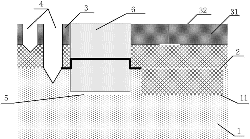
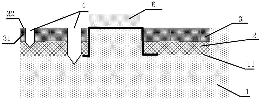
[0042] The power amplifier circuit board provided by the embodiment of the present invention can be applied to a radio base station or a high-speed transmission line such as an optical module. By adopting the integrated structure of PCB and substrate, using the substrate as the signal return path and at the same time for heat dissipation, while shortening the signal return path, it also takes into account good heat dissipation performance and reduces loss.

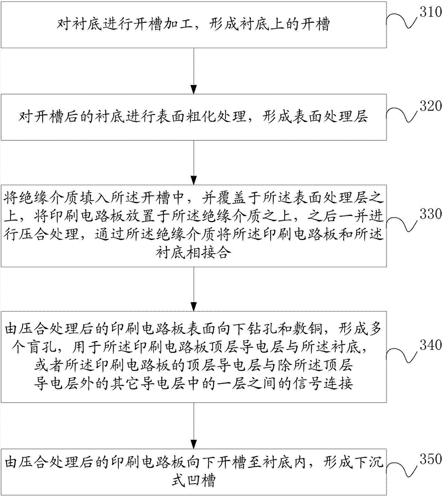
[0043] figure 1 It is a schematic diagram of a power amplifier circuit board provided by Embodiment 1 of the present invention. As shown in the figure, the power amplifier circuit board includes: a substrate 1 , an insulating medium layer 2 , a printed circuit board 3 , a blind hole 4 and a sunken groove 5 .

[0044] The substrate 1 has grooves 11, specifically, the grooves 11 with different depths can be formed by etching or machining. A surface treatment layer (not shown in the figure) is formed on the upper surface of...


PUM


Abstract

An embodiment of the invention discloses a circuit board of a power amplifier and a manufacturing method of the circuit board. The circuit board comprises a substrate, an insulation dielectric layer, a PCB (printed circuit board), blind holes and a sunken type groove, wherein a groove is formed in the substrate; a surface treatment layer subjected to roughening treatment is arranged on the upper surface of the substrate; the insulation media layer is arranged in the groove, and the surface treatment layer is covered with the insulation dielectric layer ; the PCB comprises at least one core plate; conducting layers are arranged on two sides of each core plate; the PCB is arranged on the insulation dielectric layer and is connected with the insulation dielectric layer through the bottom core plate of the PCB and the conducting layer on the lower side of the bottom core plate; the blind holes are formed between the top conducting layer and the substrate or among other conducting layers besides the top conducting layer in the PCB; conducting materials are arranged on the inner walls of the blind holes; the top conducting layer of the PCB is in signal connection with the substrate or other conducting layers besides the top conducting layer through the blind holes; and the sunken type groove is formed between the top conducting layer of the PCB and the substrate, and the bottom of the sunken type groove is located in the substrate.

Description

technical field [0001] The invention relates to the field of communication technology, in particular to a power amplifier circuit board and a manufacturing method thereof. Background technique [0002] Radio base stations (RBS) are widely used in various mobile communication fields. In order to increase the coverage of base stations, radio base stations with high output power are required. And high output power will lead to higher temperature of the power amplifier (PA), therefore, it is very important that the power amplifier has good heat dissipation performance. In addition, market-oriented mass production also requires the simplification of manufacturing cost and manufacturing process. [0003] In the prior art, the substrate of the power amplifier circuit board is manufactured separately from the printed circuit board (PCB), and the substrate is connected to the PCB by solder or conductive glue or non-conductive glue, and the substrate mainly plays a role of heat dissi...

Claims


Application Information

Patent Timeline
Patent Type & Authority Applications(China)
IPC IPC(8): H05K1/02H05K1/03H05K1/11
Inventor 黄明利
Owner HUAWEI TECH CO LTD
Why Eureka
Try Eureka