Radiation detector

A technology for radiation detectors and detection elements, which can be used in semiconductor devices, electric solid state devices, radiation control devices, etc., and can solve problems such as diagnostic obstacles

Inactive Publication Date: 2014-01-22
SHIMADZU SEISAKUSHO CO LTD
View PDF9 Cites 2 Cited by
  • Summary
  • Abstract
  • Description
  • Claims
  • Application Information

AI Technical Summary

Problems solved by technology

This linear artifact becom

Method used


Image

  • Radiation detector
  • Radiation detector
  • Radiation detector

Examples


Embodiment 1

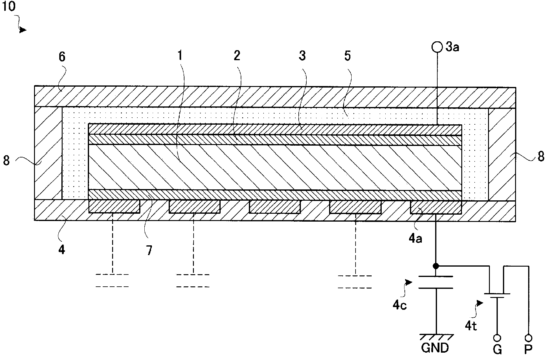
[0059] The overall structure of the X-ray detector

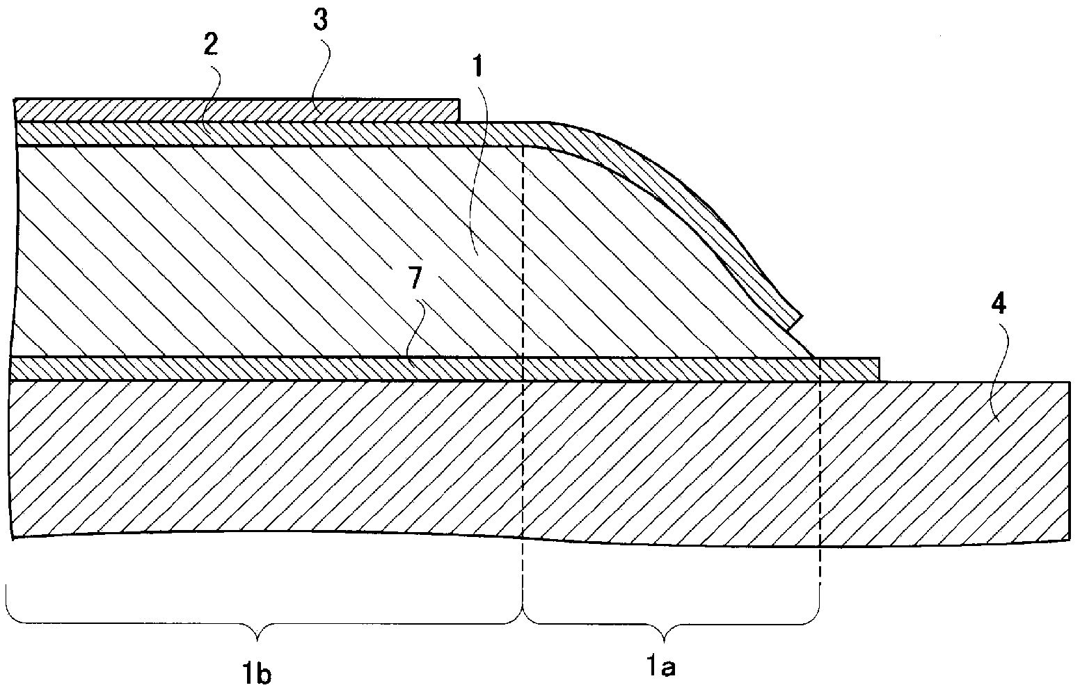
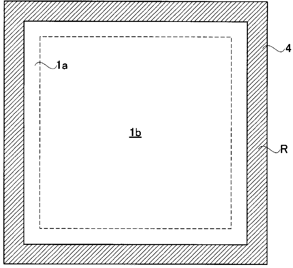
[0060] Such as figure 1 As shown, the X-ray detector 10 of Embodiment 1 has: an active matrix substrate 4, which is used to accumulate and read out the charges induced by the movement of carriers; an amorphous selenium layer 1, which is used to convert X-rays carrier pair; second high-resistance film 2; common electrode 3; epoxy resin layer 5, which is formed by curing epoxy resin at room temperature; and auxiliary plate 6, which is formed of glass. In addition, the X-ray detector 10 is configured by stacking an active matrix substrate 4, a first high-resistance film 7, an amorphous selenium layer 1, a second high-resistance film 2, a common electrode 3, an epoxy resin layer 5, and an auxiliary plate 6 in this order. . The X-ray detector corresponds to the radiation detector of the present invention.

[0061] The amorphous selenium layer 1 corresponds to the semiconductor layer of the present invention, and the second hi...


PUM

PropertyMeasurementUnit
Resistivityaaaaaaaaaa
Thicknessaaaaaaaaaa
Thicknessaaaaaaaaaa

Abstract

Provided is a radiation detector that prevents shorting of electrical wirings that intersect with an inter-layer insulating layer there between, and wherein the occurrence of detector element failure is suppressed. By means of the present configuration, an amorphous selenium layer (1) and the electrical wiring of an active matrix substrate (4) are contrived in a manner so as to not short. Namely, the electrical wiring is provided to the position at which the layer thickness of the amorphous selenium layer (1) is covered by a thick central portion. As a result, the electrical wiring is reliably isolated from an electrode layer, and so it is possible to provide a radiation detector that can withstand long-term use.

Description

technical field [0001] The present invention relates to a radiation detector for imaging radiation, and more particularly to a radiation detector whose durability is improved by suppressing the increase of defective pixels. Background technique [0002] Radiation detectors for imaging radiation are used in various fields including the medical field. The specific structure of this radiation detector will be described. Such as Figure 15 As shown, the conventional radiation detector 60 includes: an amorphous selenium layer 51, which is used to convert radiation into electron-hole carrier pairs; a high resistance film 52, a high resistance film 57, which is used to cover the amorphous selenium The two surfaces of the layer 51 are stacked; the active matrix substrate 54 is arranged in contact with the high resistance film 57, and a thin film transistor, electric wiring, and an interlayer insulating layer are formed on the glass substrate; the electrode layer 53 is stacked In t...

Claims


Application Information

Patent Timeline
IPC IPC(8): H01L27/14H01L27/146
CPCH01L27/14603H01L27/14618H01L27/14676H01L31/115H01L2924/0002H01L2924/00H01L27/14636
Inventor 佐藤贤治辻久男
Owner SHIMADZU SEISAKUSHO CO LTD
Why Eureka
Try Eureka