
Insulated gate bipolar thyristor module and electrode power terminals

A technology of power terminals and insulating gates, applied in circuits, electrical components, electrical solid devices, etc., can solve problems such as large inductance, simplify tooling and process, and eliminate inability to interconnect or complex interconnection.

Active Publication Date: 2016-04-20
ZHUZHOU CRRC TIMES SEMICON CO LTD
View PDF6 Cites 0 Cited by
  • Summary
  • Abstract
  • Description
  • Claims
  • Application Information

AI Technical Summary

Problems solved by technology

This makes the inductance introduced by the electrode power terminal larger

Method used


Image

  • Insulated gate bipolar thyristor module and electrode power terminals
  • Insulated gate bipolar thyristor module and electrode power terminals
  • Insulated gate bipolar thyristor module and electrode power terminals

Examples


Embodiment 1

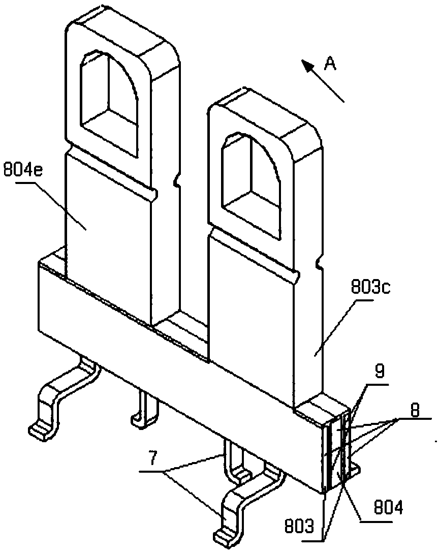
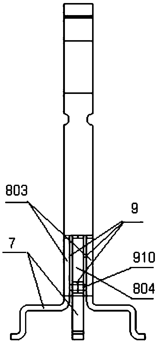
[0062] Such as figure 2 and image 3 As shown, the electrode power terminal provided in Embodiment 1 is a composite two-electrode power terminal, which includes a first electrode 803 and a second electrode 804, wherein the first electrode 803 and the second electrode 804 are composed of a multi-layer plate structure .

[0063] The multi-layer plate structure includes N (N≥3, N is a natural number) layers of electrode plates 8 , and an insulating plate 9 is spaced between two adjacent layers of electrode plates 8 . In the multi-layer board structure, the electrode plates of M (M≥2, M<N, M is a natural number) layers are electrically connected through at least one first through hole 910, so that the electrode plates of M layers constitute electrode power terminals The first electrode 803 of the first through hole 910 is separated from each of the remaining (N-M) electrode plates by an insulating layer to achieve electrical insulation. At least one electrode plate of the rema...

Embodiment 2

[0074] Such as Figure 5 As shown, the electrode power terminal provided by the second embodiment integrates three electrode layers, which are respectively the first electrode 805 , the second electrode 806 and the third electrode 807 as shown in the enlarged view on the right. This embodiment has many similarities with the first embodiment. For the sake of brevity, this embodiment focuses on the differences. For the same parts as the first embodiment, please refer to the detailed description of the first embodiment.

[0075] The difference between the electrode power terminal provided in this embodiment and the electrode power terminal provided in Embodiment 1 is that a third electrode 807 is added to the electrode power terminal in this embodiment, and a third electrode 807 is also added correspondingly. The part 807j for external connection and the third welding leg extending outward from the third electrode 807 .

[0076] Same as Embodiment 1, the electrode power terminal...

Embodiment 3

[0084] First, based on the electrode power terminals provided in the first and second embodiments above, the embodiment of the present invention provides an embodiment of a substrate layout with low parasitic inductance.

[0085] At present, in order to reduce the parasitic inductance of the power semiconductor module, in the insulated gate bipolar thyristor module, the conventional circuit layout of the liner is shown in Figure 6 (1). For the convenience of description, Fig. 6 (1) shows two substrates 2, each substrate is provided with a plurality of sub-clad copper layers 3, and each substrate 2 contains four IGBT chips 4 and corresponding FRD chips 5 . The IGBT chip 4 and the FRD chip 5 are symmetrically distributed on both sides of the electrode power terminal with respect to the center line of the lining board, and the collector of the IGBT chip 4 and the cathode of the FRD chip 5 are welded to the copper clad layer 3 of the lining board, so as to be welded to the same T...


PUM


Abstract

The present invention provides an insulated gate bipolar thyristor module and an electrode power terminal, wherein the electrode power terminal includes a first electrode and a second electrode, and the first electrode and the second electrode are composed of a multilayer board, The multi-layer board includes N-layer electrode boards, and an insulating board is arranged between two adjacent layers of electrode boards, wherein the M-layer electrode boards are electrically connected through at least one first through hole to form the first electrode, and Each of the first through holes is electrically insulated from every electrode plate except the M layer of electrode plates, and at least one layer of electrode plates other than the M layer of electrode plates constitutes the second electrode. Since the multilayer electrode plates are electrically connected through the first through holes, the alternate arrangement of the multilayer electrode plates can be realized, which can increase the area where the electrodes face each other in parallel and reduce parasitic inductance. The parasitic inductance generated by the IGBT module based on the electrode power terminal is also low.

Description

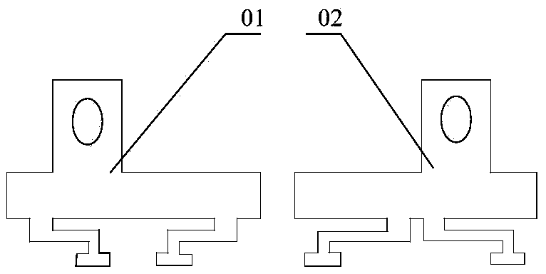
technical field [0001] The invention relates to the technical field of power electronic equipment, in particular to an insulated gate bipolar thyristor module and an electrode power terminal. Background technique [0002] In a power semiconductor module, the interconnection of chips and the extraction of electrode power terminals will bring a certain amount of parasitic inductance, which will have a negative impact on circuits and devices. [0003] Usually, the parasitic inductance inside the module is mainly determined by the circuit layout of the lining board and the structure of the electrode power terminal. Among them, the parasitic inductance generated by the electrode power terminal accounts for the main part. [0004] At present, conventional electrode power terminals such as figure 1 Shown are two parallel electrode plates 01 and 02. In order to reduce the inductance of the electrode power terminals, the distance between the two parallel electrode plates is usuall...

Claims


Application Information

Patent Timeline
Patent Type & Authority Patents(China)
IPC IPC(8): H01L23/49H01L25/18
CPCH01L2924/1301H01L2924/13055H01L2924/30107H01L2224/0603H01L2224/48091H01L2224/48137H01L2224/49111H01L2224/49113H01L2224/49175H01L2924/00014H01L2924/00
Inventor 徐凝华刘国友吴义伯窦泽春忻兰苑
Owner ZHUZHOU CRRC TIMES SEMICON CO LTD
Learn More