Circulating etching method of silicon nitride hole with high depth-to-width ratio

A high aspect ratio, silicon nitride technology, used in electrical components, circuits, semiconductor/solid-state device manufacturing, etc. eclipse effect

Active Publication Date: 2014-02-12
SOI MICRO CO LTD
View PDF6 Cites 15 Cited by
  • Summary
  • Abstract
  • Description
  • Claims
  • Application Information

AI Technical Summary

Problems solved by technology

If the polymer is too little, it is difficult to obtain the ideal etching morphology, and the selectivity is low, it is difficult to control the size of the critical dimension CD of the hole; however, if too much fluorocarbon polymer film is deposited in the deep hole, it will be harmful Sidewalls and bottom act as chemical inhibitors that cause etch to stop

Method used


Image

  • Circulating etching method of silicon nitride hole with high depth-to-width ratio
  • Circulating etching method of silicon nitride hole with high depth-to-width ratio
  • Circulating etching method of silicon nitride hole with high depth-to-width ratio

Examples


Embodiment 1

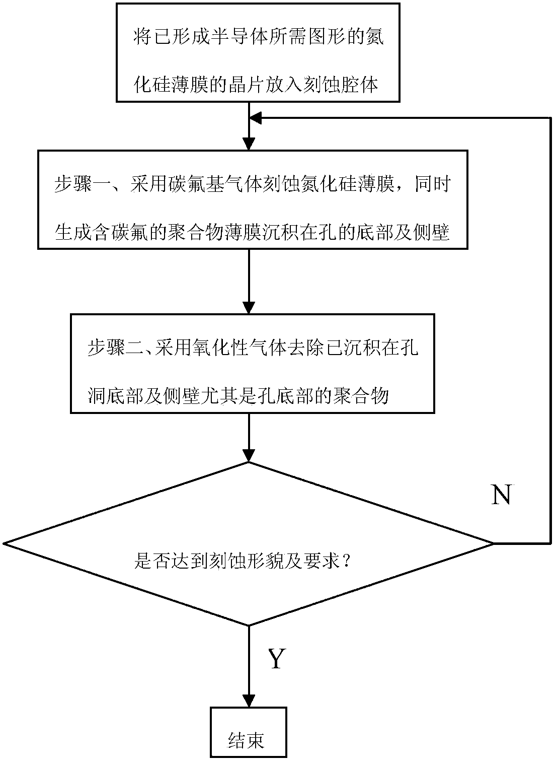
[0038] Embodiment 1. Etching a high-aspect-ratio hole with a steep shape on a single-layer silicon nitride film

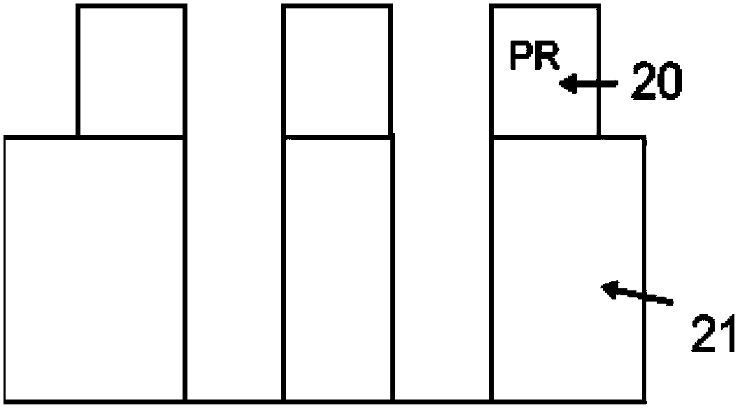
[0039] image 3 It is a cross-sectional view of a steep etch topography of a high aspect ratio hole in a single-layer silicon nitride film according to Embodiment 1 of the present invention. In this embodiment, a layer of silicon nitride film 21 is firstly deposited on the substrate on which the basic semiconductor structure has been formed, and a photoresist is used as the mask 20 (depending on the requirements of different process nodes, sometimes it may be necessary to add a hard mask touch), photolithography out of the desired pattern. Then, an etching gas is introduced into the etching chamber, excited by radio frequency power, and after the plasma is stabilized, the two-step silicon nitride etching process of the present invention is performed.

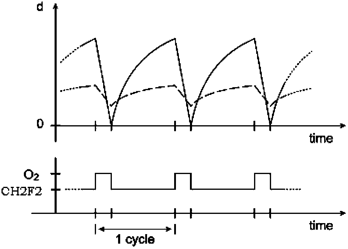
[0040] In the first embodiment, firstly, the fluorocarbon-based etching gas CH is introduced in the first step. ...

Embodiment 2

[0043] Example 2: Etching a slightly inclined high-aspect-ratio hole on a single-layer silicon nitride film

[0044] Figure 4 It is a cross-sectional view of the slightly inclined etching topography of the high aspect ratio hole of the single-layer silicon nitride film according to the second embodiment of the present invention. Because for etched holes with high aspect ratio, figure 2 The steep topography shown poses considerable challenges for subsequent filling. Sometimes for the subsequent process, it is necessary to make the size of the bottom smaller to make a slightly inclined result. Embodiment 2 is also first to use PECVD to deposit a layer of silicon nitride film 31 on the substrate on which the basic semiconductor structure has been formed, and use photoresist as the mask 30 (depending on the requirements of different process nodes, sometimes it may be necessary to add a hard film). mask), photoetching out the desired pattern. Then, an etching gas is introduce...

Embodiment 3

[0047] Embodiment 3: Etching a high aspect ratio hole on a multilayer silicon nitride film

[0048] Figure 5 The etching cross-sectional view of the high aspect ratio hole of the multilayer silicon nitride film according to the third embodiment of the present invention. Embodiment 3 Firstly, a layer of silicon nitride film 41 is deposited on the surface of the device on which a multilayer semiconductor structure has been formed, and a photoresist is used as the mask 40 (depending on the requirements of different process nodes, sometimes it may be necessary to add a hard film). mask), photoetching out the desired pattern. Then, an etching gas is introduced into the etching chamber, excited by radio frequency power, and after the plasma is stabilized, a two-step silicon nitride etching process is performed.

[0049] The process parameters can refer to the above examples. It can stop above or below the dielectric layer 42 as desired. The difference between this embodiment an...


PUM


Abstract

A circulating etching method of a silicon nitride hole with high depth-to-width ratio comprises of the steps of 1 adopting a dry-method plasma process and fluorocarbon-based gas to perform silicon nitride thin film etching so as to form the hole and meanwhile generating a polymer depositing on the bottom and the side wall of the hole; 2 feeding oxidizing gas and diluting gas into an etching cavity. The deposition amount of fluorocarbon on the side wall of the deep hole can be controlled, the polymer depositing on the bottom of the deep hole can be removed so as to ensure continuous etching, and the two steps are repeatedly performed till the etching profile of the hole meets the requirement. When the fluorocarbon-based gas in the step 1 is increased and accordingly the fluorocarbon amount is increased, the hole is slightly oblique. When the oxidizing gas in the step 2 is increased, the hole is upright. Different hole etching profiles can be obtained as required by adjusting parameters to be between the two amounts.

Description

technical field [0001] The invention belongs to the field of semiconductor integrated circuit manufacturing, and more specifically relates to a cyclic etching method for a silicon nitride film with a high aspect ratio hole. Background technique [0002] Silicon nitride is widely used in the manufacture of ultra-large-scale semiconductor integrated circuits, such as etching barrier layer, electrical insulating dielectric layer, anti-reflection layer, or as a hard mask for etching other semiconductor materials, and so on. [0003] For the hole etching of silicon oxide and silicon nitride films, fluorocarbon-based gases such as CF are generally used. 4 、CHF 3 、CH 2 f 2 、CH 3 F, C 4 f 8 For etching, the steepness of the sidewall surface is a key parameter. The control of steepness mainly lies in adjusting the amount of polymer, that is, O 2 It depends on the amount deposited on the sidewall after reacting with the fluorocarbon. For high aspect ratio hole etching, this r...

Claims


Application Information

Patent Timeline
Patent Type & Authority Applications(China)
IPC IPC(8): H01L21/311
CPCH01L21/31116
Inventor 孟令款
Owner SOI MICRO CO LTD
Why Eureka
Try Eureka