Multilayered medium etching method

A technology of multi-layer dielectric and etching gas, applied in the direction of electrical components, semiconductor/solid-state device manufacturing, circuits, etc., can solve problems such as difficult to realize, thin dielectric layer, and affect the quality of etching structure, etc., to achieve the adjustment of etching rate , the effect of increasing the etching rate

Active Publication Date: 2013-04-17
ADVANCED MICRO FAB EQUIP INC CHINA
View PDF2 Cites 5 Cited by
  • Summary
  • Abstract
  • Description
  • Claims
  • Application Information

AI Technical Summary

Problems solved by technology

[0009] However, if the etching gas for etching silicon dioxide is mechanically combined with the etching gas for etching silicon nitride and similar materials, using methods such as CF 4 、CHF 3 , O 2 , Ar mixed gas is used as an etching gas to etch multilayer dielectrics formed of different materials such as silicon dioxide, silicon nitride, and low dielectric constant materials. No matter how various gas ratios are adjusted, the above differences cannot be resolved. Fast, high-quality plasma etching of multilayer dielectrics formed of materials
The reason is that the combination of these gases has a selectivity ratio of the etching rate of silicon dioxide to the etching rate of silicon nitride and similar materials that is difficult to control near 1:1, usually the etching rate of silicon dioxide Much higher etch rate than silicon nitride
For example, for the etching of via holes formed by multi-layer dielectric materials, due to the reflection of high-energy ions near the side walls, the etching rate near the side walls will be slightly faster than that of the center of the via hole. When the etching front passes through the silicon nitride layer , if the etching front near the sidewall first touches the silicon dioxide layer of the next layer, the etching rate at this position is much higher than the etching rate at the center of the via hole, and such figure 1 The etching stop (Etching Stop) phenomenon shown in the silicon nitride dielectric material 100 etches the bottom of the via hole 101 to form a bump 102, which seriously affects the quality of the etching structure
[0010] At the same time, due to the multilayer dielectric formed by different materials such as silicon dioxide, silicon nitride, carbon-containing silicon nitride, and low dielectric constant materials in the semiconductor structure as an interlayer dielectric layer, it usually has different thicknesses at different device features. difference, and the thickness of the dielectric layer of some materials is extremely thin, it is difficult to use different etching gases for different etching process steps for the dielectric layer of different materials

Method used


Image

  • Multilayered medium etching method
  • Multilayered medium etching method
  • Multilayered medium etching method

Examples


Embodiment Construction

[0038] In order to make the purpose, technical solution and advantages of the present invention clearer, the following will further describe the implementation of the present invention in detail in conjunction with the accompanying drawings. Those skilled in the art can easily understand other advantages and effects of the present invention from the contents disclosed in this specification. The present invention can also be implemented or applied through other different specific implementation modes, and various modifications or changes can be made to the details in this specification based on different viewpoints and applications without departing from the spirit of the present invention.

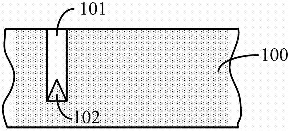
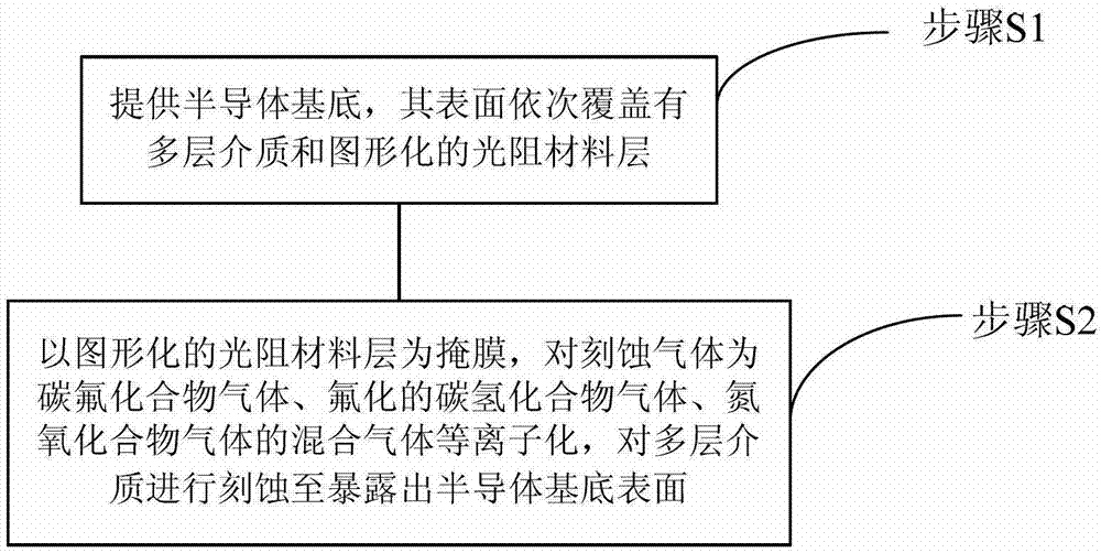
[0039] figure 2 It is a flow chart of the steps of the multilayer dielectric etching method provided by the present invention.

[0040] Such as figure 2 As shown, the multilayer dielectric etching method provided in this specific embodiment includes the following steps:

[0041] Step ...


PUM


Abstract

The invention relates to the technical field of a semiconductor, and discloses a multilayered medium etching method. The method comprises the following steps of: providing a semiconductor substrate, wherein the surface of the semiconductor substrate is sequentially coated with the multilayered medium and a graphic photoresist layer; and ionizing the etching gas which is the mixed gas such as fluorocarbon gas, fluorinated carbureted hydrogen gas and nitrogen oxide gas by taking the graphic photoresist layer as a mask, and etching the multilayered medium by the etching gas until the multilayered medium is exposed to the surface of the semiconductor substrate. The method takes the fluorocarbon gas and the fluorinated carbureted hydrogen gas with high C/F ratio as the main etching gas; and the nitrogen oxide gas in a certain flow is added, so that a purpose of etching the multilayered medium formed by different materials through one-step plasma etching primary is achieved, and the etching is not performed by many steps of layering the materials. The photoresist layer as the mask has a low etching rate.

Description

technical field [0001] The invention relates to the technical field of semiconductors, in particular to the etching technology of multi-layer dielectric structures such as interlayer dielectric layers in the semiconductor preparation process. Background technique [0002] The preparation of semiconductor integrated circuits is an extremely complicated process, the purpose of which is to prepare various semiconductor device structures and metal interconnections required by a specific circuit on a semiconductor substrate with as small an area as possible in a small size. Wherein, each semiconductor device structure must be electrically connected through appropriate metal interconnections in order to exert expected circuit functions. [0003] As the preparation of integrated circuits develops toward ultra-large-scale integrated circuits (ULSI), the structural density of semiconductor devices inside them, that is, the degree of device integration, is increasing. However, as the...

Claims


Application Information

Patent Timeline
Patent Type & Authority Applications(China)
IPC IPC(8): H01L21/311H01L21/768
Inventor 杜若昕王兆祥刘骁兵刘志强
Owner ADVANCED MICRO FAB EQUIP INC CHINA
Why Eureka
Try Eureka