Etching method for silicon nitride high depth-to-width ratio hole

A high aspect ratio, silicon nitride technology, used in electrical components, circuits, semiconductor/solid-state device manufacturing, etc., can solve problems such as low selectivity ratio, etching suspension, and difficulty in obtaining etching topography

Active Publication Date: 2014-01-22
SOI MICRO CO LTD
View PDF4 Cites 6 Cited by
  • Summary
  • Abstract
  • Description
  • Claims
  • Application Information

AI Technical Summary

Problems solved by technology

If the polymer is too little, it is difficult to obtain the ideal etching morphology, and the selectivity is low, it is difficult to control the size of the critical dimension CD of the hole; however, if too much fluorocarbon polymer film is deposited in the deep hole, it will be harmful Sidewalls and bottom act as chemical inhibitors that cause etch to stop

Method used


Image

  • Etching method for silicon nitride high depth-to-width ratio hole
  • Etching method for silicon nitride high depth-to-width ratio hole
  • Etching method for silicon nitride high depth-to-width ratio hole

Examples


Embodiment Construction

[0023] The present invention will be described in detail below in conjunction with the accompanying drawings and by taking specific implementations as examples. However, those skilled in the art should know that the present invention is not limited to the specific embodiments listed, as long as it conforms to the spirit of the present invention, it should be included in the protection scope of the present invention.

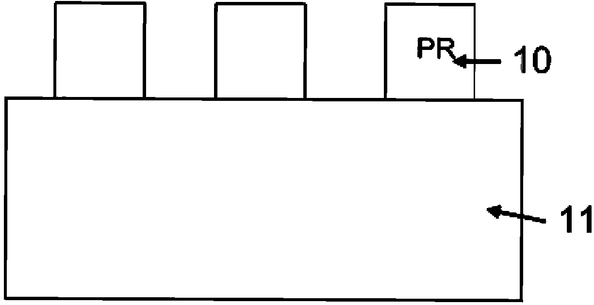
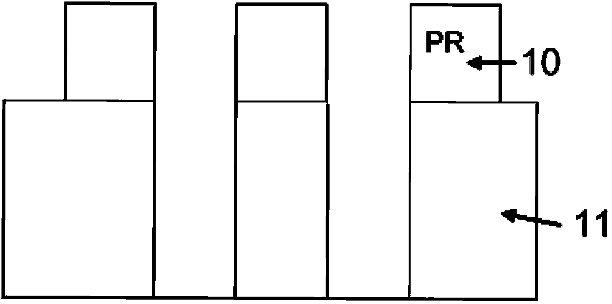
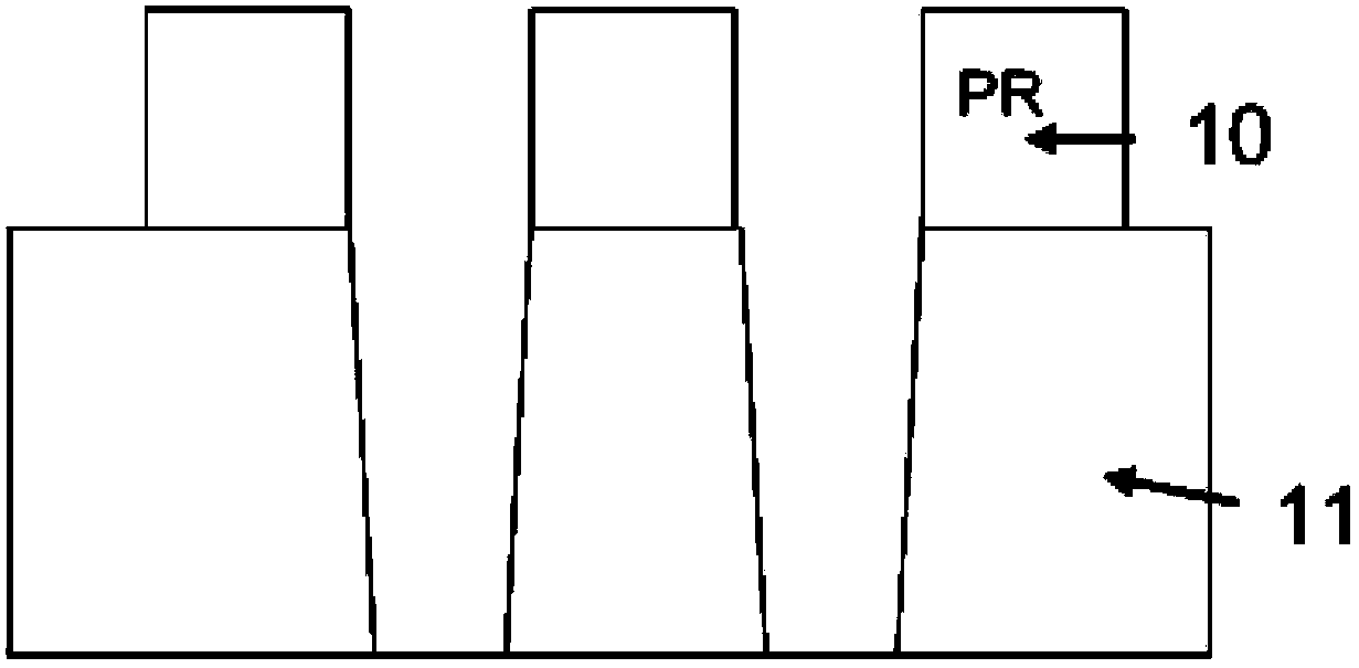
[0024] The etching method of the silicon nitride high aspect ratio hole of the present invention comprises the following steps:

[0025] First, put the silicon nitride film structure wafer with the required pattern developed by photolithography into the etching chamber; Inert gas, hydrogen-containing fluorocarbon-based gas, and radio frequency power are added to excite the plasma; after the plasma stabilization step, the silicon nitride film is etched until the etching morphology and aperture size of the high aspect ratio hole and The depth meets the requirement...


PUM


Abstract

The invention discloses an etching method for a silicon nitride high depth-to-width ratio hole. The method comprises: first of all, placing a semiconductor device of a silicon nitride film, already forming the graph needed by a semiconductor, into en etching cavity; then using a dry-method plasma technology, letting in a high carbon chain molecule fluorocarbon-based gas, an oxidizing gas, a dilution gas and a fluorocarbon-based gas containing hydrogen, adding radio frequency power and exciting plasma; and after a plasma stabilization step, performing etching of the silicon nitride film until the etching morphology, the hole diameter size and the depth of a high depth-to-width ratio hole reach requirements. According to the invention, the silicon nitride film is etched by using the unique fluorocarbon-based gas, through adjusting gas component and power size, the deposition amount of fluorocarbon polymers on the side wall of the deep hole can be controlled, the key dimensions of the hole can be prevented from becoming larger, and polymers already deposited at the bottom of the deep hole can be removed so as to ensure that the etching can be continued, thus the etching morphology of the hole can be adjusted.

Description

technical field [0001] The invention belongs to the field of semiconductor integrated circuit manufacturing, and more specifically relates to an etching method for a silicon nitride film with a high aspect ratio hole. Background technique [0002] Contact hole etching is a key technology of VLSI. As CMOS enters the technology era after 32nm, high aspect ratio hole etching and its filling have a considerable impact on the yield of devices. For advanced memories, the aspect ratio has reached more than 40:1, which makes the challenge even greater. [0003] The contact hole etching medium of traditional CMOS devices is silicon dioxide film. As another widely used dielectric material, silicon nitride is hardly used as an ILD layer due to its large K value and stress. It is mainly used as a stop layer for hard mask, etch or CMP. [0004] Similar to the etching of silicon oxide films, for silicon nitride films, fluorocarbon-based gases such as CF 4 、CHF 3 、CH 2 f 2 、CH 3 F e...

Claims


Application Information

Patent Timeline
Patent Type & Authority Applications(China)
IPC IPC(8): H01L21/311
CPCH01L21/31105H01L21/76801
Inventor 孟令款
Owner SOI MICRO CO LTD
Why Eureka
Try Eureka