Field stop type insulated gate bipolar transistor and manufacturing method thereof

A bipolar transistor and insulated gate technology, applied in the direction of transistors, semiconductor/solid-state device manufacturing, semiconductor devices, etc., can solve the problem of high cost

Inactive Publication Date: 2014-02-12
CSMC TECH FAB1
View PDF7 Cites 2 Cited by
  • Summary
  • Abstract
  • Description
  • Claims
  • Application Information

AI Technical Summary

Problems solved by technology

However, the general 600V / 1200V FS type IGBT is an ultra-thin sheet. At present, there is no domestic company that can manufacture it. However, some large foreign companies may use a full-line thin-sheet circulation technology, so the cost is very high.

Method used


Image

  • Field stop type insulated gate bipolar transistor and manufacturing method thereof
  • Field stop type insulated gate bipolar transistor and manufacturing method thereof
  • Field stop type insulated gate bipolar transistor and manufacturing method thereof

Examples


Embodiment Construction

[0046] Introduced below are some of the various embodiments of the invention, intended to provide a basic understanding of the invention. It is not intended to identify key or critical elements of the invention or to delineate the scope of protection.

[0047] In order to make the object, technical solution and advantages of the present invention clearer, the present invention will be further described in detail below in conjunction with the accompanying drawings.

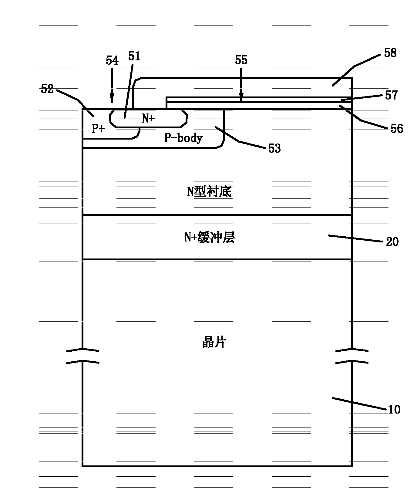
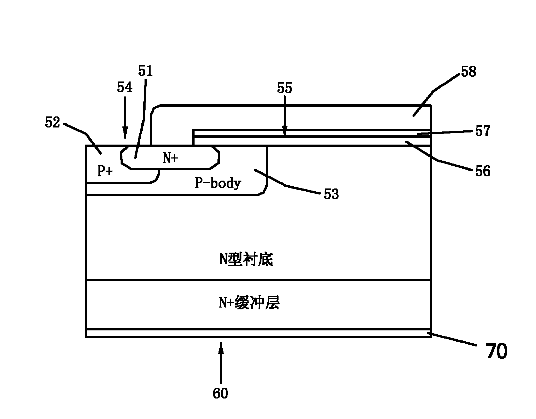
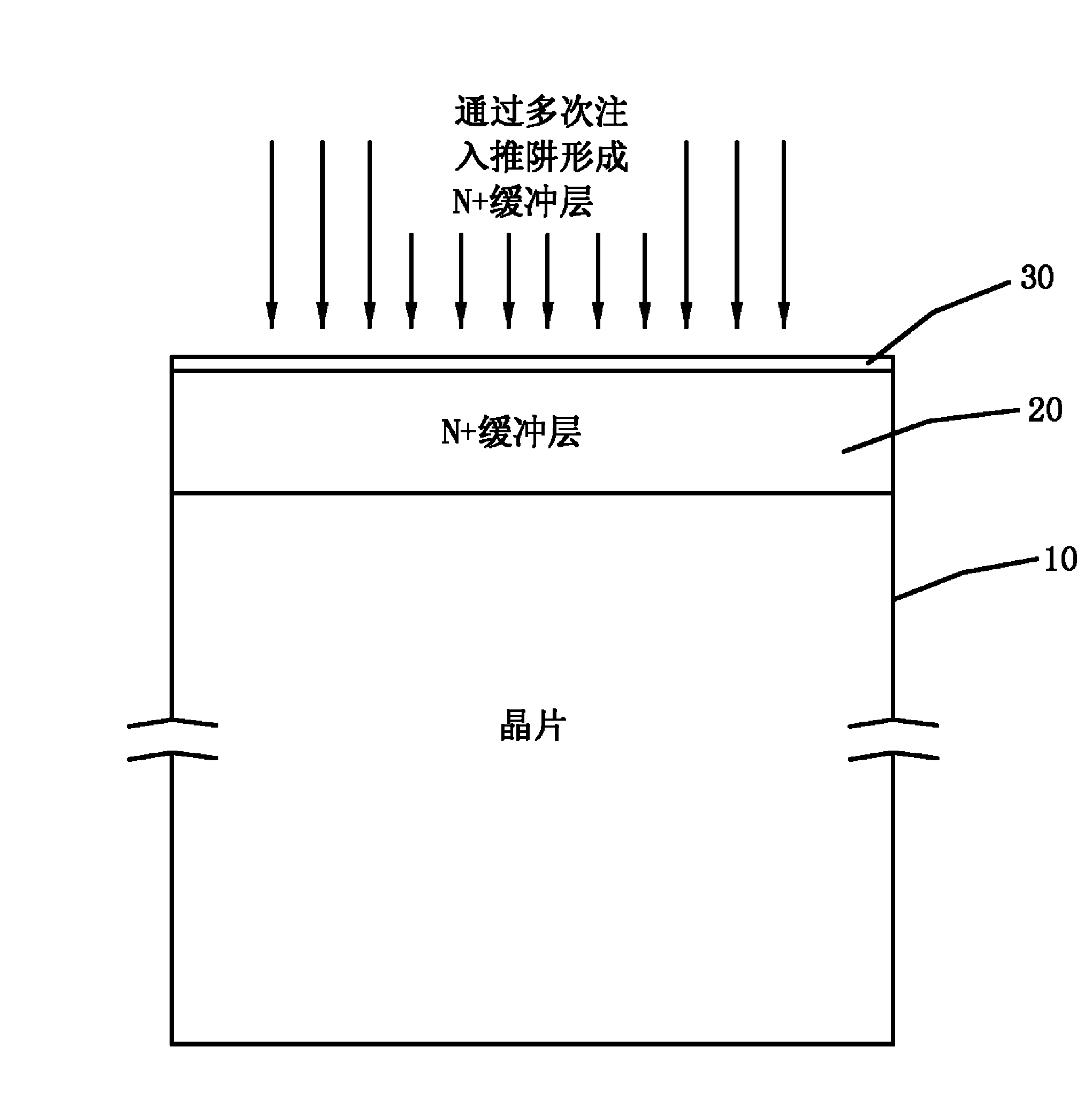
[0048] figure 1 It is a flowchart showing the main steps of the manufacturing method of the FS type insulated gate bipolar transistor of the present invention. Such as figure 1 As shown, the manufacturing method of the FS type insulated gate bipolar transistor of the present invention mainly includes: step S101 of forming a buffer layer, forming N + Buffer layer; Step S102 of forming an N-type device layer, in N + The N-type device layer is formed by epitaxial growth on the N-type buffer layer; the step S103 of...


PUM


Abstract

The invention relates to a field stop type insulated gate bipolar transistor and a manufacturing method of the field stop type insulated gate bipolar transistor. The manufacturing method of the field stop type insulated gate bipolar transistor sequentially comprises the following steps of (1) forming a buffer layer, wherein an N+ buffer layer is formed on the obverse side of a wafer; (2) forming an N-type device layer, wherein the N-type device layer is formed on the N+ buffer layer through epitaxial growth; (3) forming an IGBT structure, wherein an obverse side structure of the IGBT is formed on the N-type device layer; (4) forming a collector, wherein the collector is formed on the reverse side of the wafer. According to the manufacturing method of the field stop type insulated gate bipolar transistor, the ultra-thin field stop type insulated gate bipolar transistor can be manufactured without sheet processing equipment, the manufacturing method of the field stop type insulated gate bipolar transistor has the advantages of being simple in technology, high in efficiency and low in cost, and the field stop type insulated gate bipolar transistor manufactured through the manufacturing method of the field stop type insulated gate bipolar transistor has the lower conduction voltage drop and the lower application temperature.

Description

technical field [0001] The present invention relates to the field of integrated circuit manufacturing, in particular to a method for manufacturing a Field Stop (Field Stop, FS for short) insulated gate bipolar transistor (Insulated Gate Bipolar Transistor, IGBT for short) and a field stop manufactured by the method. Discontinued insulated gate bipolar transistor. Background technique [0002] IGBT is a composite fully-controlled voltage-driven power semiconductor device composed of BJT (bipolar transistor) and MOS (insulated gate field effect transistor), which has both high input impedance of MOSFET and low conduction voltage drop of GTR. The advantages. The saturation voltage of GTR is low, the carrying current density is large, but the driving current is large; the driving power of MOSFET is small, the switching speed is fast, but the conduction voltage drop is large, and the current carrying density is small. The IGBT combines the advantages of the above two devices, w...

Claims


Application Information

Patent Timeline
IPC IPC(8): H01L21/331H01L29/739
CPCH01L29/7395H01L29/66333H01L29/7398
Inventor 邓小社王根毅芮强吴芃芃
Owner CSMC TECH FAB1
Why Eureka
Try Eureka