
Eureka
For R&D, Eureka makes reading and utilizing patents & technical documents easy.
Eureka AIR
Designed for self-driven R&D workflows. Generate viable solutions, solve complex R&D challenges, empower your innovation with AI.

Eureka Materials
Designed for material experts only. Revolutionize your material R&D, from search, analyze, to developing new materials.

TechResearch
Generate reliable direction feasibility study reports for your R&D in just a few steps.

TechSeek
Discover and master advanced knowledge NOW. Basics, ideas, possibilities, all at once.

TechMind
As an expert in R&D Theories, TechMind can generates customized viable solutions instantly.

TechRisk
Analyze your overall solution with one click, know your potential R&D risks in advance.

TechMonitor
Get weekly tech updates, stay abreast of the latest tech innovations and key insights.
Process-compatible decoupling capacitor and method for making the same
A technology for decoupling capacitors and capacitor electrodes, which is applied in the fields of capacitors, semiconductor/solid-state device manufacturing, electric solid-state devices, etc., and can solve the problems that decoupling capacitors cannot completely meet the requirements
- Summary
- Abstract
- Description
- Claims
- Application Information
AI Technical Summary
Problems solved by technology
Method used
Image

Examples
Embodiment Construction
[0034] It should be understood that the following disclosure provides many different embodiments and examples for implementing the different features of the invention. Specific examples of components and arrangements are described below to simplify the present disclosure. Of course, these are examples only and not intended to be limiting. Furthermore, in the following description the first part is formed over or on the second part includes an embodiment in which the first and second parts are formed to be in direct contact, and may also include an embodiment in which a part is formed interposed between the first and second parts. An embodiment of an additional component so that the first and second components are not in direct contact. Various components in the drawings may be arbitrarily drawn in different scales for simplicity and clarity.
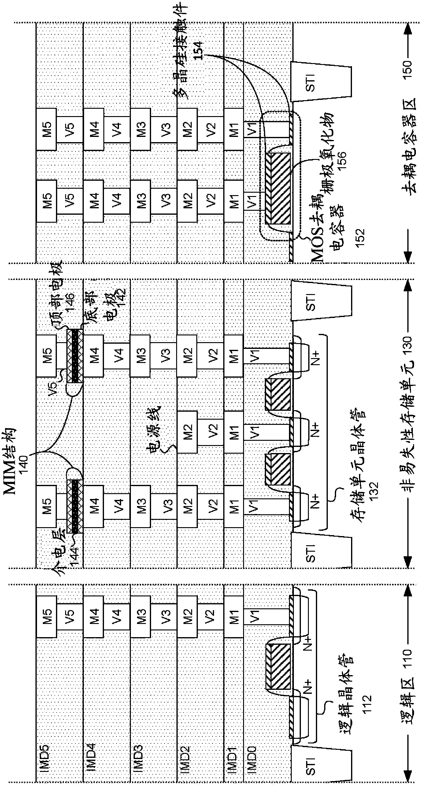
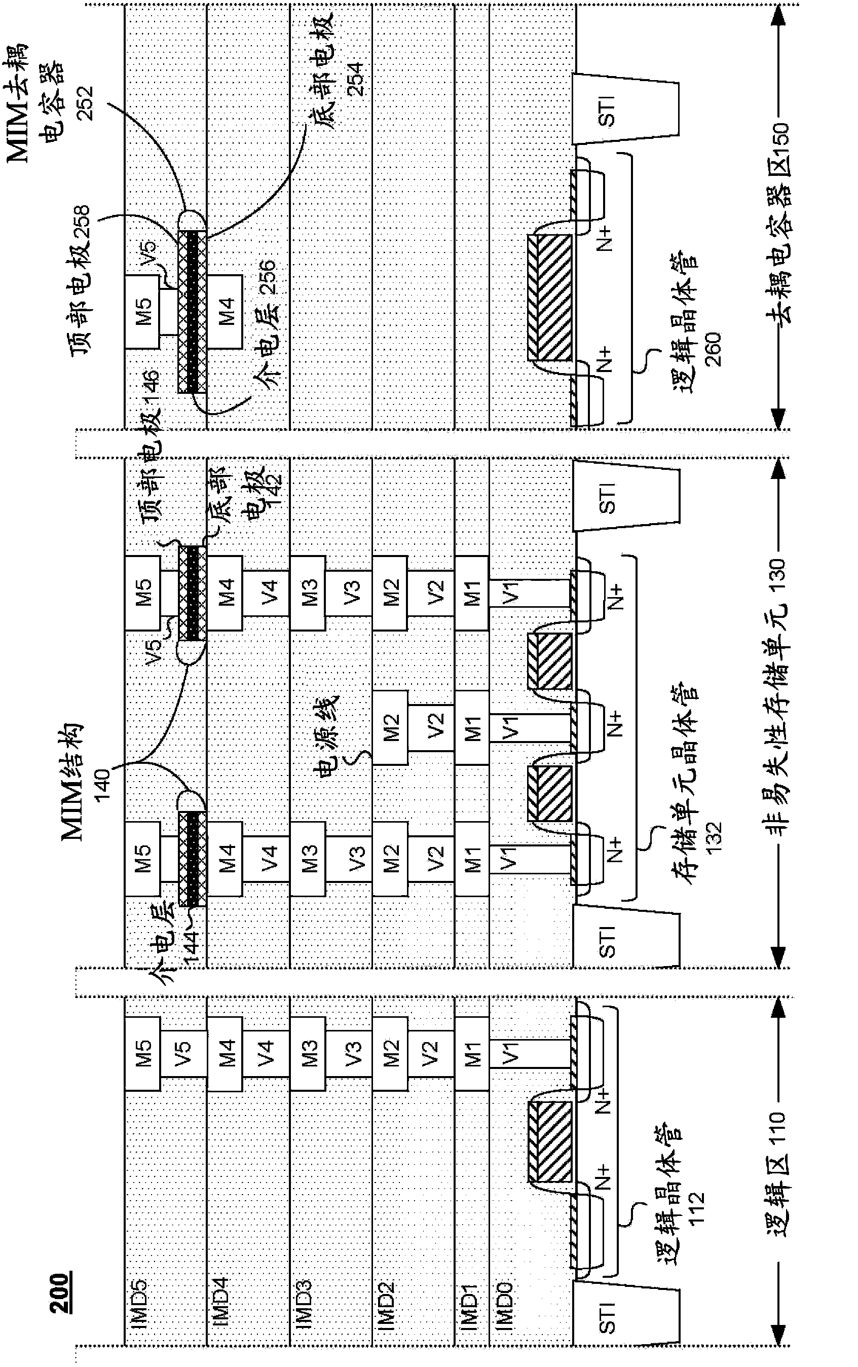
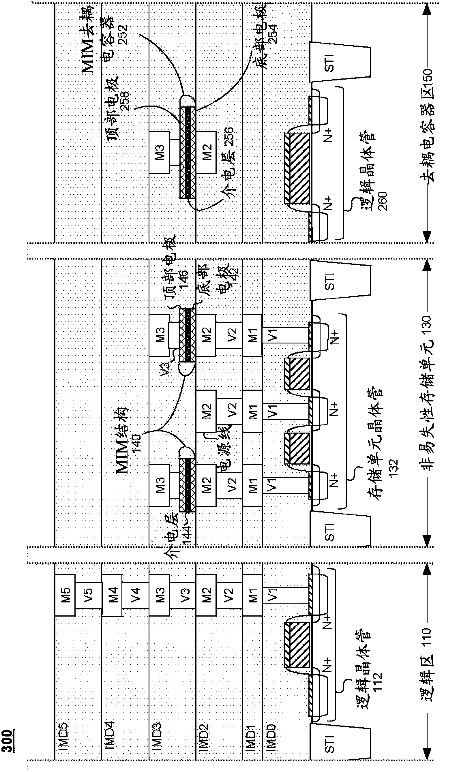
[0035] figure 1 A system-on-chip (SOC) 100 is shown, which may include multiple functional areas fabricated on a single substrate. ...
PUM
 Abstract
Description
Claims
Application Information
 - R&D Engineer
- R&D Manager
- IP Professional
- Industry Leading Data Capabilities
- Powerful AI technology
- Patent DNA Extraction
Browse by: Latest US Patents, China's latest patents, Technical Efficacy Thesaurus, Application Domain, Technology Topic, Popular Technical Reports.
© 2024 PatSnap. All rights reserved.Legal|Privacy policy|Modern Slavery Act Transparency Statement|Sitemap|About US| Contact US: help@patsnap.com