

Metal silicide, metal germanide, methods for making the same
a technology of metal germanide and metal silicide, which is applied in the direction of coating, semiconductor devices, chemical vapor deposition coating, etc., can solve the problems of low resistance silicide on the top of the gate, source, drain and any other exposed silicon surface, and process may not be effective in all contexts. , the effect of ni over the three-dimensional structure is poor
- Summary
- Abstract
- Description
- Claims
- Application Information
AI Technical Summary
Benefits of technology
Problems solved by technology
Method used
Image

Examples
example 1
[0284]Experiments were conducted using ALD of Sb for the interface layer, followed by ALD of metal oxide over the interface layer, followed by an anneal in a reducing environment that accomplished both reduction of the metal oxide and silicidation of the underlying silicon through the interface layer.
[0285]Initially, 5 cm×5 cm silicon substrates were dipped in 1% aqueous HF solution for native oxide cleaning. Sb was then deposited by ALD at 100° C. using a F-120 research scale reactor. SbCl3 and (EtsSi)3Sb were alternately pulsed with intervening purging for 100 cycles. Reactant pulse / purge lengths were 1 / 3 s for SbCl3 and 2 / 3 s for (EtsSi)3Sb. Subsequently, NiO was deposited by ALD in a Pulsar 2000 ALCVD prototype reactor at 160° C. by alternately pulsing bis(4-N-ethylamino-3-penten-2-N-ethyliminato)nickel (II) and O3. Pulse durations of 1 s and purge durations of 4 s were used for both reactants, and 2000 cycles were performed. Post-deposition annealing was conducted for 1 minute...
example 2
[0287]Experiments were conducted using epitaxial Ge for the interface layer, followed by ALD of metal oxide over the interface layer, followed by an anneal in a reducing environment that accomplished both reduction of the metal oxide, germanidation of the interface layer and silicidation of the underlying silicon through the interface layer.
[0288]Continuous Ge films with thickness from about 7 to about 15 nm were deposited by CVD on silicon at 350° C. by using deposition times from about 150 seconds to about 210 seconds. Surface roughnesses of the Ge films were about 0.6 nm. NiO was deposited by ALD in a Pulsar 2000 ALCVD prototype reactor at 160° C. by alternately pulsing bis(4-N-ethylamino-3-penten-2-N-ethyliminato)nickel (II) and O3. Pulse durations of 1 s and purge durations of 4 s were used for both reactants, and 2000 cycles were performed. Post-deposition annealing was conducted for 10 minutes at 450° C. in 1 atmosphere partial pressure of forming gas (5% / 95% H2 / N2).
[0289]Cry...
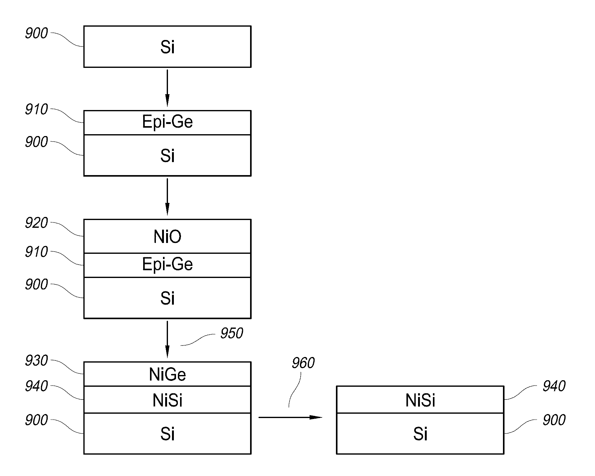
example 3
[0290]Experiments were conducted using epitaxial Ge films on Si of 1 μm in thickness followed by ALD of metal oxide over the Ge film, followed by an anneal in a reducing environment that accomplished both reduction of the metal oxide and germanidation of the underlying germanium.
[0291]NiO was deposited by ALD in a Pulsar 2000 ALCVD prototype reactor at 160° C. by alternately pulsing bis(4-N-ethylamino-3-penten-2-N-ethyliminato)nickel (II) and O3. Pulse durations of 1 s and purge durations of 4 s were used for both reactants, and 2000 cycles were performed. In-situ XRD was done using an HTK 1200N oven commercially available from Anton Paar GmbH of Österich, Austria, and the PANalytical X'PERT PRO MPD diffractometer in forming gas (5 / 95% H2 / N2) up to 600° C.
[0292]FIG. 9 illustrates the results of the x-ray diffraction (XRD) analyses, showing composite images for annealing the nickel oxide over germanium at different temperatures. The NiO reflections disappear at 250° C., and NiGe begi...
PUM
| Property | Measurement | Unit |
|---|---|---|
| Thickness | aaaaa | aaaaa |
| Thickness | aaaaa | aaaaa |
| Structure | aaaaa | aaaaa |
Abstract
Description
Claims
Application Information