High intensity temperature change-resistant crimping diode

A technology of diodes and Schottky diodes, which is applied in the field of crimping diodes and can solve problems such as plastic deformation of solder

Active Publication Date: 2014-02-12
ROBERT BOSCH GMBH
View PDF4 Cites 0 Cited by
  • Summary
  • Abstract
  • Description
  • Claims
  • Application Information

AI Technical Summary

Problems solved by technology

This causes the flux to start plastically deforming

Method used


Image

  • High intensity temperature change-resistant crimping diode
  • High intensity temperature change-resistant crimping diode
  • High intensity temperature change-resistant crimping diode

Examples


Embodiment Construction

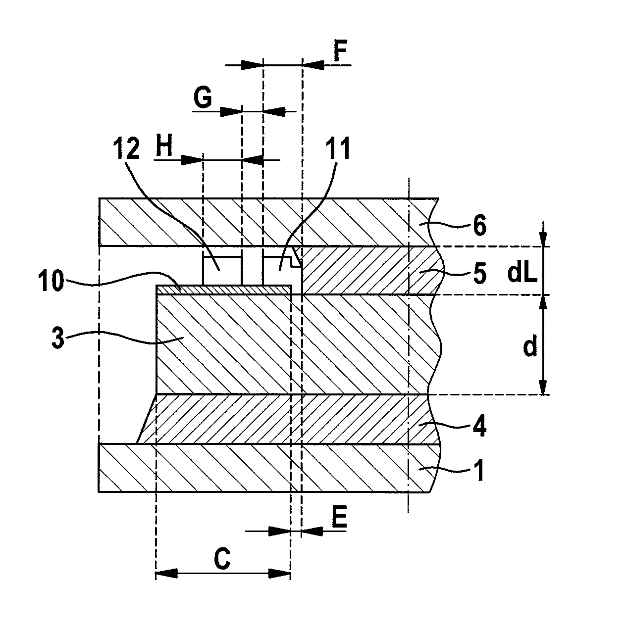
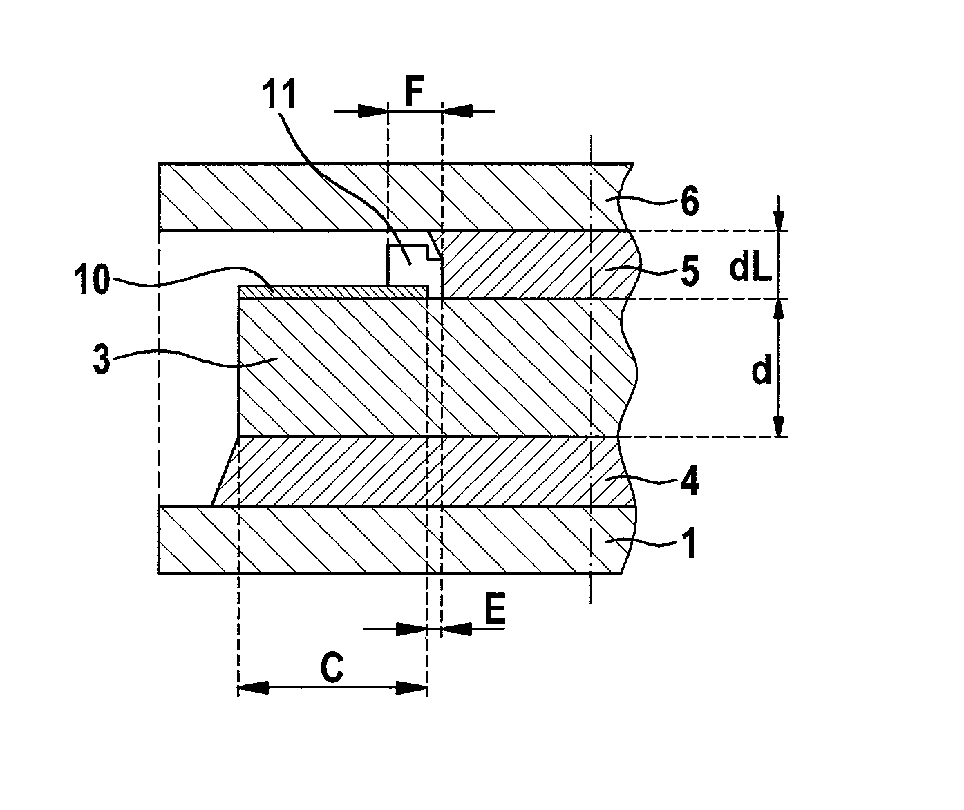
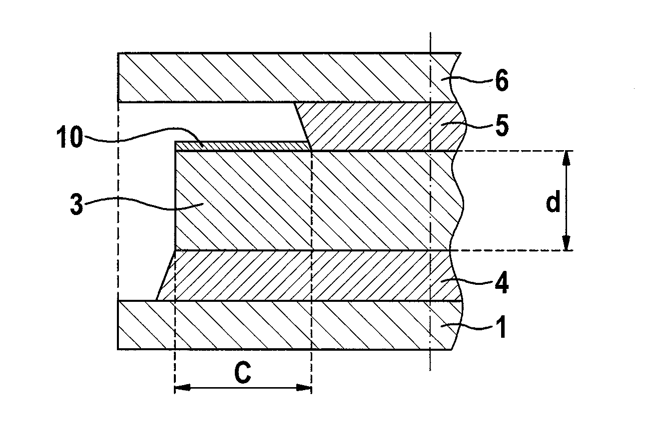
[0020] The inventors have recognized that when making crimped diodes, as in image 3 As can be seen in , the solder layer 5 is squeezed through the insulating layer 10 . this is in Figure 4 shown in the Figure 4 It can be seen that the flux layer 5 has overlapped the insulating layer 10 by a distance (C-D) after the soldering process, where C is the creep distance of the flux without overlapping and D is the The creeping distance of the flux in the case of connection. As a result of the overlap, a reduction of the creeping path occurs, by which reduction the temperature resistance of known crimp diodes is reduced.

[0021] The overlapping of the solder layer 5 on the insulating layer 10 can be traced to various causes. Among the causes are, for example, the pressure exerted on the top wire during soldering, deviations during the soldering process (Streuungen), the base 1 or the top wire 6 (cf. figure 1 ) of the surface quality fluctuations. Furthermore, there is the po...


PUM


Abstract

The invention relates to a crimping diode provided with a semisonductor chip fixed between a pedestal and a top metal wire through a connecting layer; the connecting layer contracts at least on the front surface of the chip relative to the outer rim of the chip; an area without the connecting layer on the semiconductor chip is provided with surrounded and insulated first plastic layer; furthermore, a complete surrounded and insulated second plastic layer is employed to connect an end portion in a radial direction of the first plastic layer.

Description

technical field [0001] The invention relates to a high-strength and temperature-resistant crimping diode. Such diodes are particularly suitable as diodes for use in motor vehicle generator systems. Background technique [0002] PN diodes made of silicon are mostly used in motor vehicle generator systems for the rectification of alternating current or three-phase current. Usually these diodes are mounted in special housings - so-called crimp housings, e.g. from figure 1 visible in . In this case, the crimp diode has a crimp seat 1 provided with knurling, which is crimped into a corresponding recess of a rectifier arrangement. In this case, the crimp base simultaneously takes over the permanent thermal and electrical connection of the rectifier diode to the rectifier arrangement. The crimp mount has a fastening region to which a semiconductor chip 3 is fixed, for example by means of a solder 4 . In this case, the upper side and the lower side of the semiconductor chip 3 a...

Claims


Application Information

Patent Timeline
Patent Type & Authority Applications(China)
IPC IPC(8): H01L29/872H01L23/31H01L23/488
CPCH01L2924/13052H01L2224/32245H01L29/1608H01L2224/27013H01L2224/32014H01L24/32H01L2224/8384H01L23/051H01L23/3192H01L2924/12032H01L23/3171H01L29/8725H01L2924/1033H01L2224/291H01L24/33H01L2924/10272H01L29/0619H01L2224/29116H01L2224/04026H01L2224/26145H01L2224/33181H01L24/29H01L2224/06181H01L29/2003H01L2924/12036H01L2924/10253H01L29/872H01L2224/83051H01L24/01H01L2924/014H01L2924/00
Inventor R.斯皮茨A.戈尔拉奇T.克努普弗
Owner ROBERT BOSCH GMBH
Why Eureka
Try Eureka