LED packaging method

A technology of LED packaging and LED chips, which is applied in the direction of electrical components, circuits, semiconductor devices, etc., can solve the problems of slow heat conduction, long manufacturing process time, and energy consumption, so as to reduce LED manufacturing costs, shorten manufacturing process time, reduce The effect of time spent

Inactive Publication Date: 2014-02-12
桂林机床电器有限公司
View PDF4 Cites 3 Cited by
  • Summary
  • Abstract
  • Description
  • Claims
  • Application Information

AI Technical Summary

Problems solved by technology

There are many defects in the LED packaging method in the prior art, such as uneven distribution of phosphor powder in the powder paste, which will lead to color chromatic aberration, yellow spots, and inconsistent light patterns when actually applied to lamps; at the same time, Heating is used in the encapsulation curing s

Method used


Image

  • LED packaging method

Examples


Embodiment Construction

[0018] The principles and features of the present invention are described below in conjunction with the accompanying drawings, and the examples given are only used to explain the present invention, and are not intended to limit the scope of the present invention.

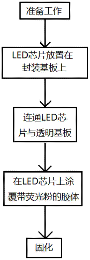
[0019] Such as figure 1 As shown, a kind of LED encapsulation method, first make preparations, make transparent substrate, heat-conducting reflective spacer, and reflective cup is arranged on the transparent substrate; Composed of a transparent substrate and a heat-conducting gasket, the heat-conducting reflective gasket is placed on the bottom of the reflective cup of the transparent substrate, and the LED chip is placed on the heat-conducting and reflective gasket; then, the LED chip and the transparent substrate are connected, and one end of the wire is welded to the LED chip On the other hand, solder the other end of the wire to the bottom of the reflective cup, so that the LED chip is connected to the transpare...


PUM

PropertyMeasurementUnit
Wavelengthaaaaaaaaaa

Abstract

The invention relates to an LED packaging method. The LED packaging method comprises the following steps that (1) a transparent substrate and a heat-conducting light-reflecting gasket are manufactured, and a light-reflecting cup is arranged on the transparent substrate; (2) the heat-conducting light-reflecting gasket is arranged at the bottom of the light-reflecting cup of the transparent substrate, and an LED chip is arranged on the heat-conducting light-reflecting gasket; (3) one end of a wire is welded to the LED chip, and the other end of the wire is welded to the bottom of the light-reflecting cup so that the LED chip and the transparent substrate can be in conduction; (4) powder slurry is formed by fluorescent powder and colloid, after stir is carried out, the powder slurry directly coats the LED chip, the transparent substrate is placed into a centrifuge, and the fluorescent powder sinks to the bottom of the colloid through powerful centrifugal force generated through high-speed rotation of a rotor of the centrifuge; (5) an infrared irradiator directly irradiates the LED chip so that the colloid can be solidified. According to the LED packaging method, consistency between the color temperature and the emitting color is ensured, and the time consumed in the process of LED packaging and solidification can be effectively and greatly reduced.

Description

technical field [0001] The invention relates to a semiconductor packaging method, in particular to an LED packaging method. Background technique [0002] LED (Light Emitting Diode), a light-emitting diode, is a solid-state semiconductor device that can directly convert electricity into light. It has the characteristics of small size, low power consumption, long service life, high brightness, environmental protection, and durability. There are many defects in the LED packaging method in the prior art, such as uneven distribution of phosphor powder in the powder paste, which will lead to color chromatic aberration, yellow spots, and inconsistent light patterns when actually applied to lamps; at the same time, Heating is used in the encapsulation curing step, which not only consumes energy, but also has a relatively slow heat conduction speed, and it takes a lot of time to complete the curing action of the curing layer, resulting in an extremely long overall LED manufacturing p...

Claims


Application Information

Patent Timeline
IPC IPC(8): H01L33/48H01L33/50
CPCH01L33/005H01L33/50
Inventor 李文礼周泰武彭应光万文华
Owner 桂林机床电器有限公司
Why Eureka
Try Eureka