COG (Chip On Glass) bonding method and temperature control device

A technology of temperature control equipment and binding area, which is applied in the direction of temperature control, optics, and instruments using electric methods, which can solve the problems of temperature contradiction, inability to detect, and inability to obtain expansion, so as to eliminate internal stress and improve quality. , the effect of a good user experience

Inactive Publication Date: 2014-02-19
BEIJING BOE OPTOELECTRONCIS TECH CO LTD
View PDF6 Cites 16 Cited by
  • Summary
  • Abstract
  • Description
  • Claims
  • Application Information

AI Technical Summary

Problems solved by technology

[0004] Due to the different expansion coefficients of the IC 12 and the glass panel 10, the edge glass of the glass panel 10 will be warped and deformed during the COG bonding process; after the bonding is completed, there will be internal stress inside the IC 12, and this problem is generally Unable to detect in the initial stage of the product
According to the prior art, the curing temperature of the ACF 13 located between the IC 12 and the glass panel 10 is generally about 200 degrees, therefore, it is necessary to develop a low-temperature ACF 13, and the temperature of the newly developed low-temperature ACF 13 is also about 150 degrees, so , there is a contradiction in temperature, and the same expansion cannot be obtained

Method used


Image

  • COG (Chip On Glass) bonding method and temperature control device
  • COG (Chip On Glass) bonding method and temperature control device
  • COG (Chip On Glass) bonding method and temperature control device

Examples


Embodiment Construction
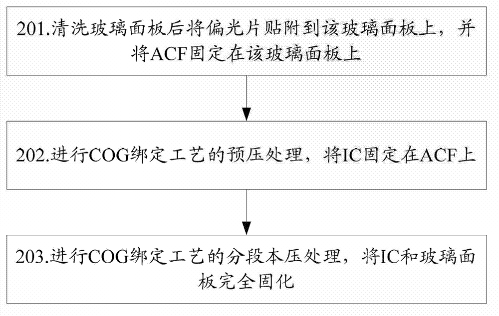
[0027]The basic idea of ​​the present invention is: after cleaning the glass panel, attach the polarizer to the glass panel, and fix the ACF on the glass panel; carry out the pre-pressing treatment of the COG binding process, and fix the IC on the glass panel On the ACF: carry out the staged pressure treatment of the COG bonding process to completely cure the IC and the glass panel.

[0028] The present invention will be further described in detail below with reference to the accompanying drawings and specific embodiments.

[0029] The invention provides a COG binding method, figure 2 It is a schematic flow diagram of the method for realizing COG binding in the present invention, such as figure 2 As shown, the method includes the following steps:

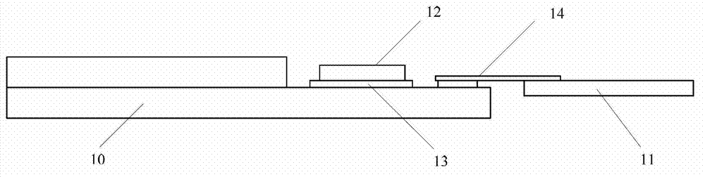
[0030] Step 201, after cleaning the glass panel, attach the polarizer to the glass panel, and fix the ACF on the glass panel;

[0031] Specifically, the glass panel 10 is first cleaned to remove foreign matter on the surface of...


PUM


Abstract

The invention discloses a COG (Chip On Glass) bonding method. The COG bonding method comprises attaching a Polaroid to a glass panel after the glass panel is cleaned and fixing an ACF (Anisotropic Conductive adhesive Film) on the glass panel; performing the pre-bonding treatment of the COG bonding process and fixing an IC (Integrated Circuit) on the ACF; performing the segment main bonding treatment of the COG bonding process and performing the complete curing on the IC and the glass panel. The invention also provides a temperature control device. According to the technical scheme of the COG bonding method and the temperature control device, the process of the COG bonding process is achieved through the segment main bonding process and accordingly the IC and the glass panel can have the same swelling amount and accordingly the badness can be avoided.

Description

technical field [0001] The invention relates to a manufacturing process of a liquid crystal display device, in particular to a COG (Chip On Glass, chip fixed on a glass substrate) binding method and temperature control equipment. Background technique [0002] figure 1 is a schematic cross-sectional view of a liquid crystal display panel in the prior art, such as figure 1 As shown, the liquid crystal display panel mainly includes a glass panel 10, a PCB (Printed Circuit Board, printed circuit board) 11, an IC (Integrated Circuit, integrated circuit board) 12, etc., generally using the COG bonding (Bonding) method, and through the ACF ( Anisotropic Conductive adhesive Film) 13 connects glass panel 10 and IC 12 , PCB 11 and glass panel 10 are connected through FPC (Flexible Printed Circuit, flexible circuit board) 14 . [0003] Along with the user's requirements for product quality, the designer's demanding on the edge area of ​​the glass panel 10, and the cost control of the...

Claims


Application Information

Patent Timeline
Patent Type & Authority Applications(China)
IPC IPC(8): G02F1/13G05D23/19
Inventor 刘俊国于洪俊王升龙君
Owner BEIJING BOE OPTOELECTRONCIS TECH CO LTD
Why Eureka
Try Eureka