Optical proximity correction method

A technology of optical proximity correction and exposure graphics, which is applied in optics, originals for photomechanical processing, instruments, etc., and can solve problems such as distortion, deformation, and complex pattern of the mask plate

Active Publication Date: 2014-02-19
SEMICON MFG INT (SHANGHAI) CORP
View PDF4 Cites 12 Cited by
  • Summary
  • Abstract
  • Description
  • Claims
  • Application Information

AI Technical Summary

Problems solved by technology

However, with the development of semiconductor technology, the patterns on the reticle in the photolithography process are becoming more and more complex.
Especially for two-dimensional mask patterns, existing optical proximity correction methods can only find a small amount of deformation and distortion in the exposure pattern corresponding to the mask pattern

Method used


Image

  • Optical proximity correction method
  • Optical proximity correction method
  • Optical proximity correction method

Examples


Embodiment Construction

[0015] In order to make the above objects, features and advantages of the present invention more comprehensible, specific implementations of the present invention will be described in detail below in conjunction with the accompanying drawings.

[0016] In the following description, specific details are set forth in order to provide a thorough understanding of the present invention. However, the present invention can be implemented in many other ways than those described here, and those skilled in the art can make similar extensions without departing from the connotation of the present invention. Accordingly, the invention is not limited to the specific implementations disclosed below.

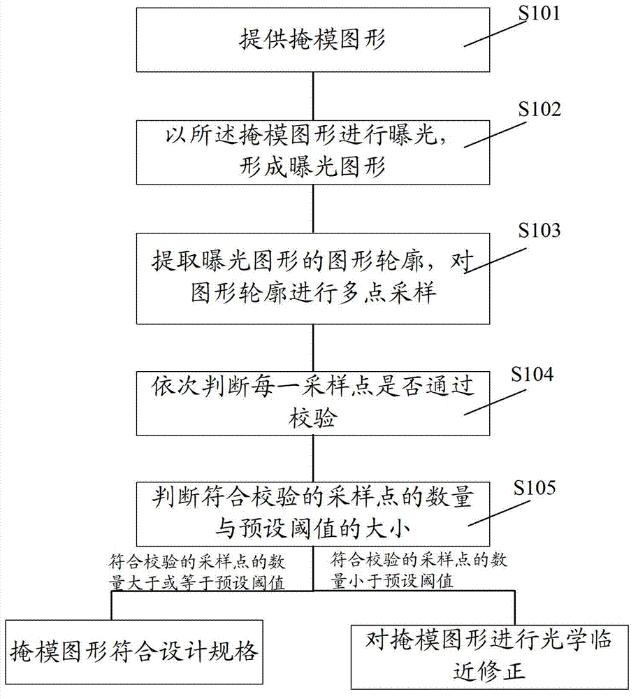
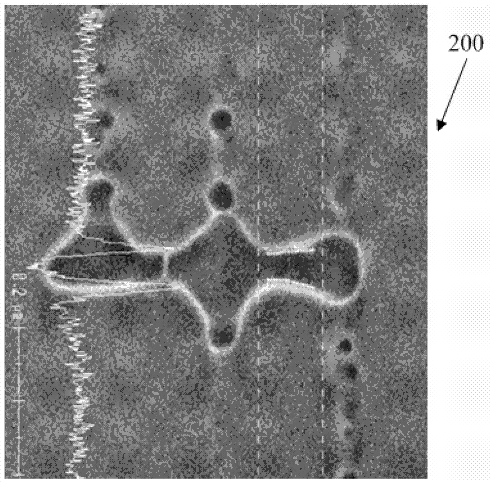
[0017] The optical proximity correction method in the prior art is to check and correct several specific points of the entire exposure pattern, and the precision of the optical proximity correction is low.

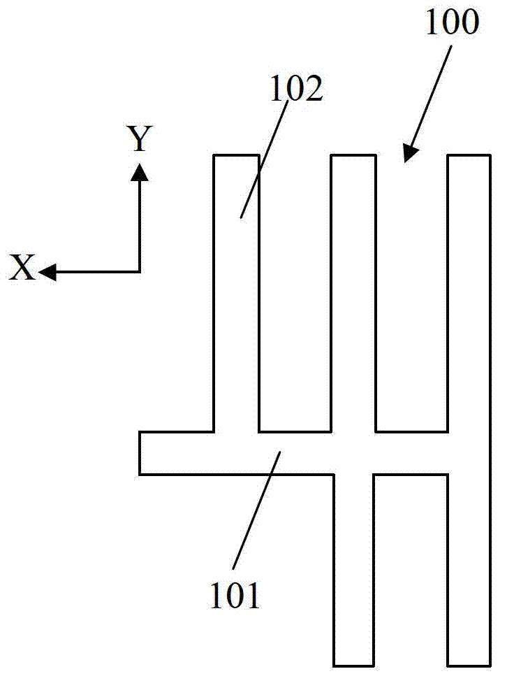
[0018] The optical proximity method provided by the present invention extracts the ent...


PUM


Abstract

An optical proximity correction method includes the steps of: a mask pattern is provided; the mask pattern is subjected to exposure to form an exposure pattern; contour of the exposure pattern is extracted, and the contour of the exposure pattern is subjected to multi-point sampling; whether each sampling point passes verification is determined successively; and the number of sampling points satisfied the verification and a preset threshold are determined; if the number of sampling points satisfied the verification is equal to or greater than the preset threshold, the mask pattern meets the design specifications; and if the number of sampling points satisfied the verification is less than the preset threshold, the mask pattern is corrected. The optical proximity correction method provided by the invention has high precision.

Description

technical field [0001] The invention relates to a semiconductor manufacturing process, in particular to an optical proximity correction method. Background technique [0002] A reticle is an essential device in the photolithography process of integrated circuit manufacturing. The mask plate mainly includes a transparent glass substrate, and a pattern to be exposed made of non-transparent material (usually chromium) covered on the glass substrate. During photolithography, the reticle is placed between the radiation source and the focusing lens, and the light emitted by the radiation source passes through the reticle, passes through the lens, and then irradiates on the wafer with photoresist spin-coated on the surface, so that the light on the wafer surface The resist layer is selectively exposed to map the pattern on the mask onto the photoresist layer. [0003] When the light emitted by the radiation source passes through the reticle, it is refracted and scattered by the ed...

Claims


Application Information

Patent Timeline
Patent Type & Authority Applications(China)
IPC IPC(8): G03F1/36
Inventor 王辉
Owner SEMICON MFG INT (SHANGHAI) CORP
Why Eureka
Try Eureka