Positioning nanoimprint lithography system for preparation of patterned substrate by utilizing AFM (Atomic Force Microscope) probe

A technology of nanoimprinting and graphic substrates, which is applied in the photoplate-making process, optomechanical equipment, optics, etc. High positioning accuracy, strong repeatability, and improved integration

Active Publication Date: 2014-02-19
INST OF SEMICONDUCTORS - CHINESE ACAD OF SCI
View PDF4 Cites 2 Cited by
  • Summary
  • Abstract
  • Description
  • Claims
  • Application Information

AI Technical Summary

Problems solved by technology

At present, the more respected quantum dot preparation process is based on the pattern substrate positioning technology, but the pattern substrate prepared by the tra

Method used


Image

  • Positioning nanoimprint lithography system for preparation of patterned substrate by utilizing AFM (Atomic Force Microscope) probe

Examples


Embodiment Construction

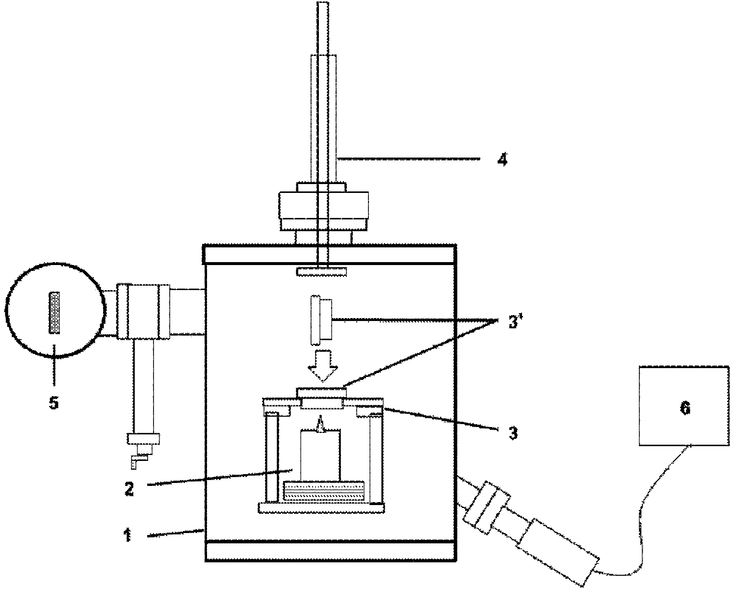
[0019] see figure 1 As shown, the present invention provides a positioning nanoimprinting system utilizing AFM probes to prepare patterned substrates, the system comprising:

[0020] An ultra-high vacuum chamber 1 compatible with other vacuum growth equipment. The vacuum degree 1 of the ultra-high vacuum chamber is generally about 1E-8 to 1E-10 Torr, which is conducive to maintaining the cleanliness of the epitaxial substrate, and corresponding adjustments can be made according to the vacuum epitaxy equipment connected thereto. The vacuum chamber is connected to other vacuum equipment through a flange, and the diameter of the flange is based on the premise that the substrate holder 3' can be transferred between chambers;

[0021] An atomic force microscope 2 is fixed on the bottom of the ultra-high vacuum chamber 1 . The atomic force microscope 2 is a redesigned atomic force microscope with imprinting function, the direction of the probe is upward, and the probe is generally...


PUM


Abstract

The invention provides a positioning nanoimprint lithography system for preparation of a patterned substrate by utilizing an AFM (Atomic Force Microscope) probe. The positioning nanoimprint lithography system comprises an ultrahigh vacuum chamber compatible with other vacuum growth equipment, an AFM fixed at the bottom of the ultrahigh vacuum chamber, a substrate holder fixing device fixed on the AFM, a substrate holder positioned in a hole formed in the middle of the substrate holder fixing device, a mechanical arm fixed on the ultrahigh vacuum chamber and used for transmitting of the substrate holder, a probe replacement cavity fixed in the side wall of the ultrahigh vacuum chamber and used for replacement of the probe of the AFM, and a monitoring system used for control to the preparation of the imprinted patterned substrate by the AFM. The positioning nanoimprint lithography system has the characteristics of high patterned substrate precision (more than 50 nm), small extension damage, capability of facilitating preparation of high-integration-level arrays of photoelectronic devices and the like.

Description

technical field [0001] The invention belongs to the technical field of semiconductor materials and devices, and relates to a positioning nanoimprinting system for preparing pattern substrates using AFM probes. Background technique [0002] The rapid development of information technology has put forward higher and higher requirements for the integration of optoelectronic devices. The development of traditional microelectronic processes such as electron beam exposure has gradually expanded the minimum size of the process to the order of tens of nanometers, and the size of traditional passive devices has also increased. has entered the sub-micron level. However, the preparation of small-sized (about 100nm) active optoelectronic devices is still a great difficulty, mainly limited by the precision of microelectronics technology and the influence of mechanical damage on the active area of ​​optoelectronic devices. The fabrication process of low-damage devices is especially necess...

Claims


Application Information

Patent Timeline
IPC IPC(8): G03F7/00
Inventor 査国伟牛智川倪海桥尚向军贺振宏
Owner INST OF SEMICONDUCTORS - CHINESE ACAD OF SCI
Why Eureka
Try Eureka