An OLED display device packaging method and packaging structure

A packaging method and display device technology, applied in the OLED display field, can solve the problems of OLED display device damage, expensive equipment, inconvenient promotion and application, etc., and achieve the effects of fast filling rate, less bubbles, and reduced complexity and cost

Inactive Publication Date: 2016-01-20
SICHUAN CCO DISPLAY TECH
View PDF5 Cites 0 Cited by
  • Summary
  • Abstract
  • Description
  • Claims
  • Application Information

AI Technical Summary

Problems solved by technology

[0003] The common packaging method of OLED display devices is to apply sealant on the edge of the cover plate and stick it to the substrate, and then cure the sealant to complete the package. Although this sealing method can provide good mechanical strength, it fails to give the panel Provide sufficient and reliable water and oxygen barrier performance; frit glass frit sealing has better sealing performance than sealant, and can maintain sealing performance within 7000h at 85°C and 85% relative humidity, but because glass is a brittle material, packaging Cracks are prone to occur during the process, and the technical difficulty is high; in addition, for the packaging of large-size OLED display devices, the substrate and cover are easily deformed by gravity and external force, and the deformed substrate and cover are easy to touch the OLED display device OLED The cathode of the component and cause damage to the OLED display device. Although this problem can be solved by the thin-film packaging method of alternate deposition of organic materials and inorganic materials, this packaging method is complicated in process and expensive in equipment, which is not convenient for popularization and application.

Method used


Image

  • An OLED display device packaging method and packaging structure
  • An OLED display device packaging method and packaging structure
  • An OLED display device packaging method and packaging structure

Examples


Embodiment Construction

[0026] In order to make the object, technical solution and advantages of the present invention clearer, the present invention will be further described in detail below in conjunction with the accompanying drawings and embodiments. It should be understood that the specific embodiments described here are only used to explain the present invention, not to limit the present invention.

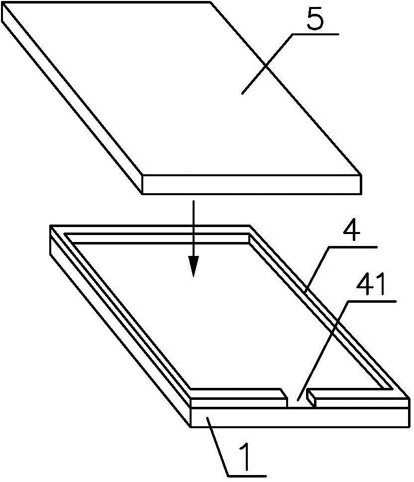
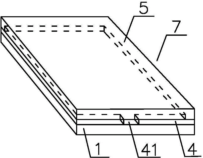
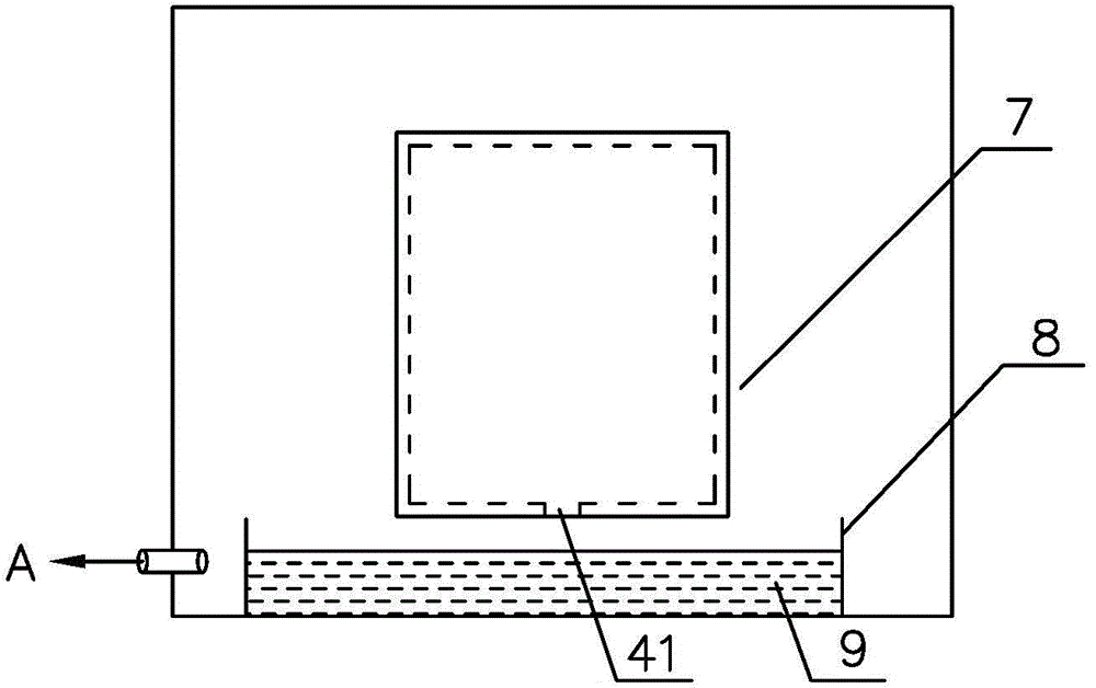
[0027] Such as Figure 4 As shown, the packaging structure of the OLED display device in this embodiment includes a substrate 1, an OLED element 2 located on the surface of the substrate 1, an insulating barrier layer 3 disposed on the surface of the OLED element 2, and an opening disposed on the edge of the substrate 1. The non-closed sealant 4, the cover plate 5 and the filling compound 6, wherein the non-closed sealant 4 bonds the substrate 1 and the cover plate 2 to form an OLED panel cavity with an opening, and the filling compound 6 fills the cavity of the OLED panel and fill the cavity of t...


PUM


Abstract

The invention discloses a packaging method and packaging structure of an OLED display device. The packaging structure comprises a substrate, an OLED component placed on the surface of the substrate, an insulating blocking layer arranged on the surface of the cathode of the OLED component, unclosed cofferdam glue arranged on the edge of the substrate, a cover plate and padding glue. The substrate and the cover plate are bonded together by the unclosed cofferdam glue to form an OLED panel cavity with an opening, the padding glue is filled into the OLED panel cavity, so that the OLED panel cavity is full of the padding glue, and the OLED component is sealed. Water vapor and / or oxygen can be blocked by the padding glue and the cofferdam glue together, and thus the packaging structure of the OLED display device has a good water-oxygen blocking property. Meanwhile, based on the pressure difference principle, the packaging method can better overcome the defect of the padding glue on one hand, on the other hand, glue filling efficiency can be better improved, and the packaging efficiency of the OLED display device is improved.

Description

technical field [0001] The invention belongs to the field of OLED display technology, and in particular relates to a packaging method and a packaging structure of an OLED display device. Background technique [0002] Organic Light-Emitting Diode (OLED) has the characteristics of all solid state, active luminescence, high brightness, high contrast, ultra-thin and ultra-light, low power consumption, no viewing angle limitation, wide operating temperature range, etc., and is considered to be the next generation The core technology of the flat panel display. However, the electrodes and organic materials constituting the OLED elements of the OLED display device are extremely sensitive to external environmental factors such as oxygen and moisture. In actual use, the OLED display device needs to be packaged to isolate the OLED element from water and oxygen to prolong the life of the OLED display device. service life. [0003] The common packaging method of OLED display devices is...

Claims


Application Information

Patent Timeline
Patent Type & Authority Patents(China)
IPC IPC(8): H01L27/32H01L51/52H01L51/56
Inventor 唐凡陈珉邹成
Owner SICHUAN CCO DISPLAY TECH
Why Eureka
Try Eureka