Method for preparing patterned doped crystalline silicon thin film for solar cells

A solar cell and thin film preparation technology, applied in the field of solar cell material preparation, can solve the problems of limiting device structure and adjustable range of process conditions, increasing the complexity of process control, and being unfavorable to solar cell performance, so as to reduce storage time, Wide selection range, energy saving effect

Active Publication Date: 2016-10-26
NANCHANG UNIV
View PDF5 Cites 0 Cited by
  • Summary
  • Abstract
  • Description
  • Claims
  • Application Information

AI Technical Summary

Problems solved by technology

High-temperature diffusion doping will lead to the interdiffusion of different doping elements of the pn junction, forming a slowly changing junction structure; and it will affect the performance of the device structure prepared before the high-temperature diffusion step
Increases the complexity of process control, limits the adjustable range of device structure and process conditions, and is not conducive to the improvement of solar cell performance

Method used


Image

  • Method for preparing patterned doped crystalline silicon thin film for solar cells
  • Method for preparing patterned doped crystalline silicon thin film for solar cells
  • Method for preparing patterned doped crystalline silicon thin film for solar cells

Examples


Embodiment 1

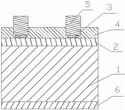
[0019] Such as figure 1 The crystalline silicon solar cell using the patterned doped silicon film as the selective emitter is prepared according to the following steps:

[0020] 1) Phosphorus (or boron) is diffused on the single crystal silicon wafer 1, and then the surface impurity layer is removed to obtain a lightly doped n-type crystalline silicon thin film emitter 2; vapor deposition method can also be used to deposit doped silicon on the single crystal silicon wafer 1. Doped silicon thin film and modified by subsequent treatment process to obtain lightly doped n-type crystalline silicon thin film emitter 2 (deposited by PECVD method, process parameters are: source gas flow rate SiH 4 :PH 3 :H 2 = 1sccm:0.2 sccm:100 sccm, deposition pressure 35 Pa, power density 0.2W / cm 2 , substrate temperature 240 o C, the deposition thickness is 200 nm; after the deposition, use H 2 protection carried out 1050 o C, 20s rapid heat treatment modification);

[0021] 2) Depositing a...

Embodiment 2

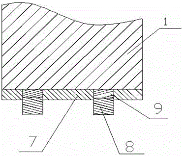
[0026] Such as figure 2 The regionalized back electric field of the crystalline silicon solar cell shown is obtained by the following process:

[0027] 1) A patterned mask plate is used to cover the surface of the single crystal silicon wafer (1), and a PECVD method is used to deposit a heavily doped patterned silicon film 9 on the back surface with a film thickness of 40 nm.

[0028] 2) The prepared heavily doped patterned silicon film 9 is crystallized by a rapid heat treatment process, and the doping elements in it are activated, and the heat treatment temperature is 1300 o C, the time is 5 s.

[0029] 3) Depositing a back surface passivation layer 7 on the exposed silicon wafer surface except the area covered by the heavily doped silicon film;

[0030] 4) Printing and sintering of the back electrode 8: the printing of the electrode should be able to cover the regionalized heavily doped crystalline silicon film, and the two should form a good ohmic contact.

Embodiment 3

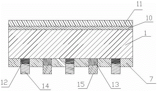
[0032] Such as image 3 The shown back crystalline silicon solar cell is prepared as follows:

[0033] 1) Deposit back electric field silicon film 12 (thickness: 30nm) and emitter silicon film 13 (thickness: 100nm) on single crystal silicon wafer 1 sequentially using different masks; the alignment between the two templates must be accurate to ensure The resulting two types of films cover the entire back surface and do not interfere with each other. The mask plate is processed according to the design requirements, and the material is stainless steel;

[0034] 2) Rapid heat treatment crystallization of the emitter film 13 and the silicon film 12 in the back electric field, using Ar gas protection, for 1050 o C, 20s rapid heat treatment modification;

[0035] 3) The passivation layer 7 on the back surface is deposited by using a mask to cover the area of ​​the emitter and the back electric field, and the deposited passivation layer needs to cover all areas except the emitter a...


PUM

PropertyMeasurementUnit
thicknessaaaaaaaaaa
thicknessaaaaaaaaaa

Abstract

The invention provides a preparation method of a patterned doped crystalline silicon thin film for a solar cell. The preparation method is characterized in that a patterned doped amorphous silicon or microcrystalline silicon thin film is prepared first by adopting a low-temperature vapor deposition technology, and then a patterned doped crystalline silicon thin film is acquired by adopting a method of rapid thermal processing. The preparation method provided by the invention can acquire richer pattern styles, and can regulate the thickness of the doped thin film, the variety of doping elements and the distribution of the doping concentration more conveniently, thereby providing space for further improving the structure and the process of crystalline silicon solar cell devices.

Description

technical field [0001] The invention relates to a method for preparing a solar cell material, in particular to a method for preparing a patterned doped crystalline silicon film for a solar cell. Background technique [0002] Solar power generation is one of the most important renewable and clean energy utilization methods for human beings. Among them, crystalline silicon solar cells have attracted widespread attention due to their abundant raw material sources and relatively mature preparation technologies, and are the mainstream product category of solar cells. [0003] The device structure of crystalline silicon solar cells has been continuously optimized and improved, from the simplest pn junction structure to various new structures such as selective emitter, selective back electric field, and back junction cells. Among the various structures mentioned above, the thin layer of doped silicon mainly depends on the high-temperature diffusion process. For example, the prepa...

Claims


Application Information

Patent Timeline
Patent Type & Authority Patents(China)
IPC IPC(8): H01L31/18
CPCH01L31/1824H01L31/202H01L31/208Y02E10/545Y02P70/50
Inventor 黄海宾周浪高江崔冶青
Owner NANCHANG UNIV
Why Eureka
Try Eureka