

Materials and methods for OLED microcavities and buffer layers
A buffer layer and microcavity technology, applied in the field of materials and methods for OLED microcavity and buffer layer
- Summary
- Abstract
- Description
- Claims
- Application Information
AI Technical Summary
Problems solved by technology
Method used
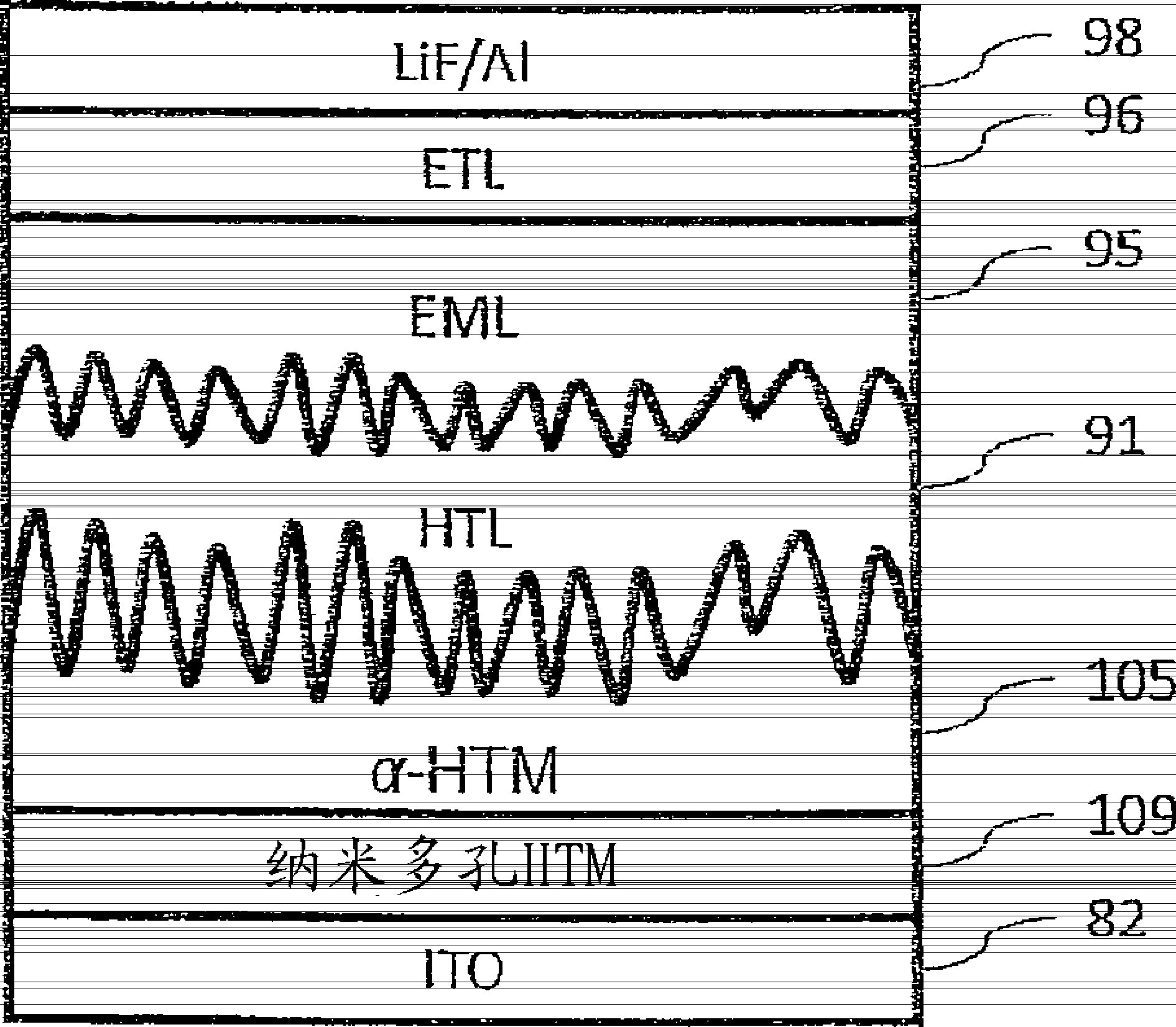
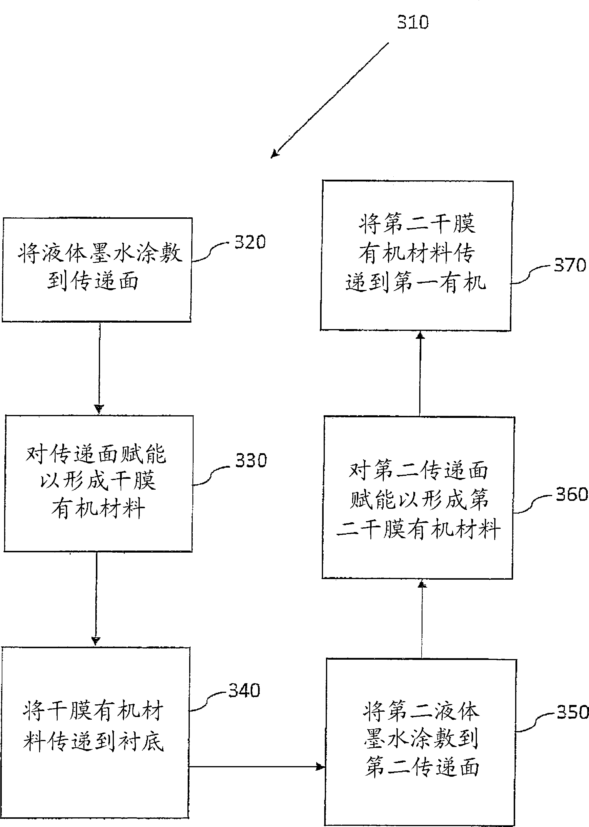
Image

Examples
example 1
[0142] This example demonstrates the functionality and excellent properties of the OLED component and the method of producing an OLED component according to the present teaching. For a 100 nm thick film, 2 drops of ink (approximately 12 picoliters) were applied at 1.2% ink concentration at 100 Hz. The loading temperature was 150°C. A vaporization temperature of about 250° C. is used over a period of time from about 200 milliseconds to about 1.0 seconds. The solids were then evaporated using a temperature ramp of 250°C - 380°C over a period of time from approximately 200 milliseconds to 800 milliseconds. A purge temperature of 350°C to 900°C is then used. The printing pitch is about 50 μm. The deposited film appeared hazy and had an AFM surface roughness greater than 5.0 nm. The printed film was post-baked at from about 150°C to about 200°C for from about 10 seconds to about 5.0 minutes on a hot plate in a nitrogen atmosphere. Atomic force microscopy (AFM) data confirmed t...
PUM
| Property | Measurement | Unit |
|---|---|---|
| Conductivity | aaaaa | aaaaa |
| Surface roughness | aaaaa | aaaaa |
| Surface roughness | aaaaa | aaaaa |
Abstract
Description
Claims
Application Information