

Chip concurrent test system
A technology of chips and chip arrays, applied in the field of chip co-testing systems, can solve the problems of increased test costs and high costs, and achieve the effect of reducing test costs, reducing expensive costs, and being easy to implement
- Summary
- Abstract
- Description
- Claims
- Application Information
AI Technical Summary
Problems solved by technology
Method used
Image

Examples
Embodiment Construction
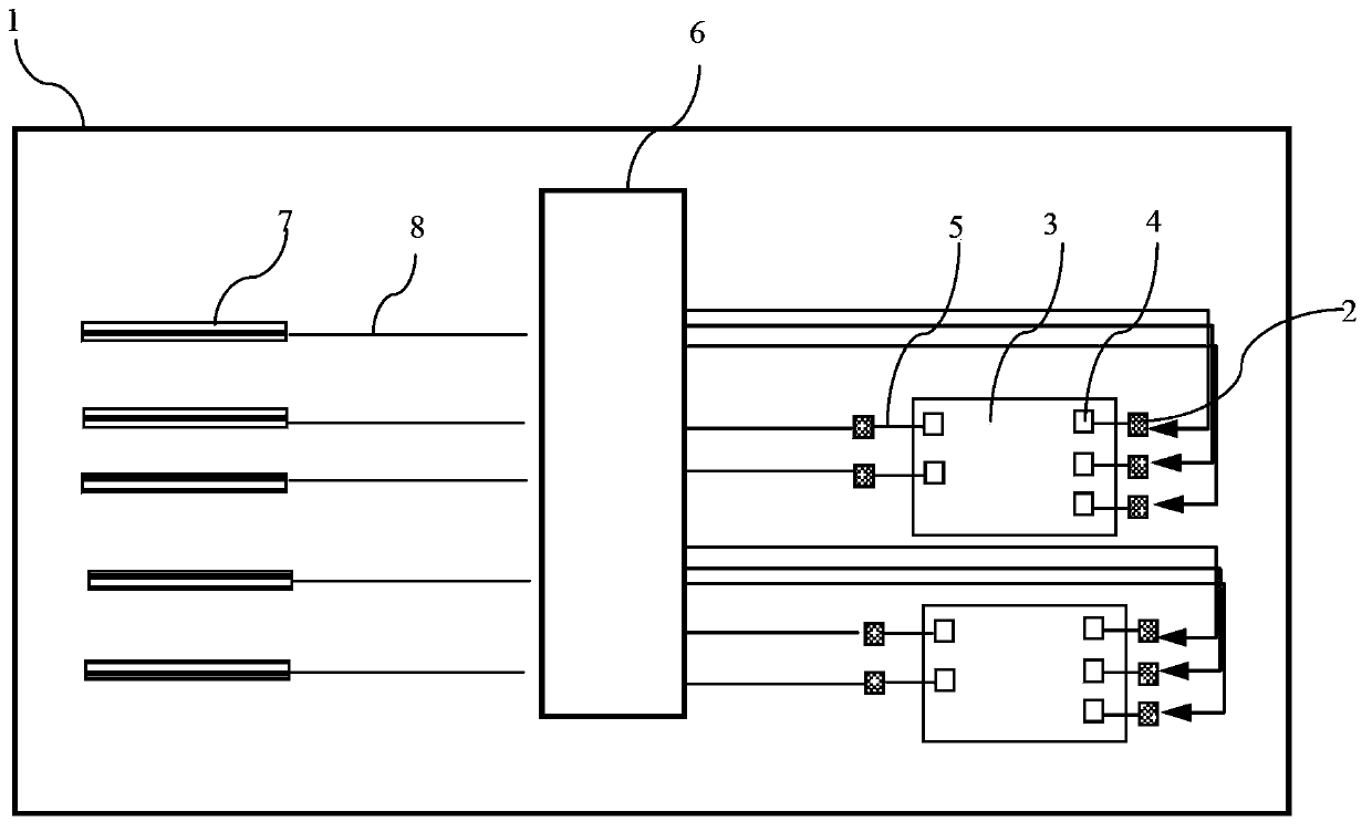
[0016] Such as figure 1 As shown, it is a schematic diagram of the chip simultaneous testing system of the embodiment of the present invention; the chip simultaneous testing system of the embodiment of the present invention includes:
[0017] A module board 1, the module board 1 is a module-level printed circuit board; a chip placement position is provided on an area of the module board 1, and the chip placement position is used for placing multiple chip arrays.
[0018] Welding pad one 2 is formed on the periphery of the chip placement position, and the position and quantity of the welding pad one 2 are set according to the position and quantity of the welding pad two 4 of the chip 3 to be tested, and the welding pad one 2 is used for Connect with the pad 2 4 .
[0019] The chip to be tested 3 is placed on the chip position by bonding, the chip to be tested 3 is a bare chip formed by cutting a wafer, and the bonding pad one 2 and the bonding pad two 4 are directly connecte...
PUM
 Abstract
Description
Claims
Application Information