Integrated circuit full-chip electro static discharge protection method and circuit

An electrostatic discharge protection and electrostatic discharge technology, applied in the field of ESD protection design and integrated circuit ESD protection design, can solve problems such as the decline of ESD capability, and achieve the effect of improving ESD capability and reducing voltage drop.

Inactive Publication Date: 2014-03-19
BEIJING CEC HUADA ELECTRONIC DESIGN CO LTD
View PDF4 Cites 9 Cited by
  • Summary
  • Abstract
  • Description
  • Claims
  • Application Information

AI Technical Summary

Problems solved by technology

In the ESD design practice of integrated circuits, engineers often find that when a proven ESD structure in a small-scale circuit is transplanted to a large-scale integrated circuit with multiple pins, the ESD capability will often be greatly reduced. This is because the long-term caused by parasitic resistance of the power line

Method used


Image

  • Integrated circuit full-chip electro static discharge protection method and circuit
  • Integrated circuit full-chip electro static discharge protection method and circuit

Examples


Embodiment Construction

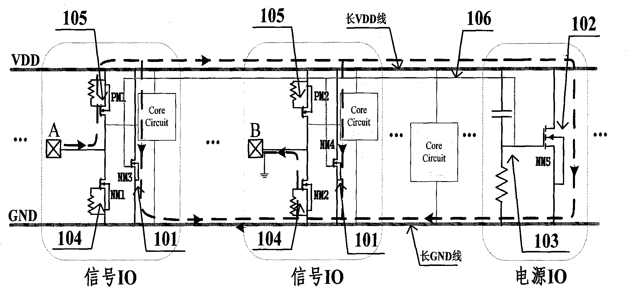
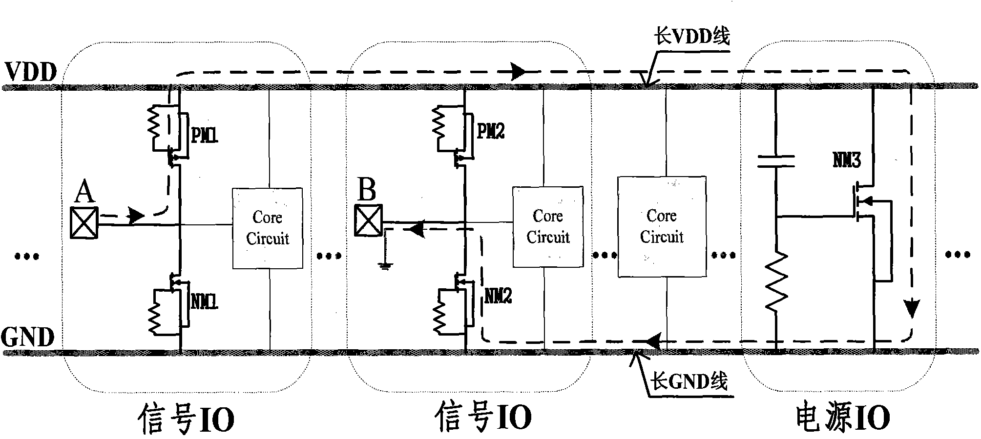
[0013] Generally, there are global power lines and ground lines in the integrated circuit, and all signal IOs and power / ground IOs are connected between the power / ground lines. The ESD test includes IO-VDD, IO-GND, IO-IO, and VDD-GND. Taking the IO-IO test as an example, when the +ESD test is performed on IO A and IO B is grounded, the electrostatic discharge current is as follows: figure 1 , 2 The discharge path shown by the arrow in the middle curve, in the traditional ESD design, the current flows through A->PM1->long VDD line->NM3->long GND line->NM2->B (ground). In large-scale integrated circuits, VDD lines and GND lines are generally long, and their parasitic resistance can reach more than 4 ohms. The on-resistance of an ESD device is about 5 ohms. For HBM2000V testing, its discharge current is about 1.33A. In traditional ESD design , the voltage drop of the discharge loop of this circuit can reach more than 30V, that is, the A node voltage in the IO unit exceeds 30V, w...


PUM


Abstract

The invention is an integrated circuit full-chip electro static discharge (ESD, Electro Static Discharge) protection method. According to an integrated circuit full-chip ESD structure of the method, one power-ground ESD discharge path is added in each signal IO unit, namely, a full chip not only contains an electro static discharge path 102 in a power IO unit, but also contains the electro static discharge path 101 in each signal IO unit. Therefore, the number of the electro static discharge paths in the full chip is increased, the electro static discharge path between IO is shortened, the discharge resistance between IO is reduced, the full-chip electro static discharge efficiency is improved, and the full-chip ESD level is upgraded.

Description

technical field [0001] The invention is applicable to the field of integrated circuit ESD protection design, especially for large-scale integrated circuits with multiple pins, and is suitable for the ESD protection of nano-process integrated circuits with more fragile device structures and lower failure voltages and integrated circuits with higher ESD requirements. design. Background technique [0002] As the integrated circuit (IC: integrated circuit) manufacturing process level has entered the deep submicron era and nanometer era, the MOS transistors in the integrated circuit adopt the lightly doped structure LDD (Lightly Doped Drain); the silicide covers the diffusion area of ​​the MOS transistor Above; the polycrystalline compound process is used to reduce the series resistance of the gate polysilicon; and the thickness of the gate oxide layer of the MOS transistor is getting thinner and the channel length is getting smaller and smaller. These improvements have improved...

Claims


Application Information

Patent Timeline
Patent Type & Authority Applications(China)
IPC IPC(8): H02H9/04
Inventor 李志国
Owner BEIJING CEC HUADA ELECTRONIC DESIGN CO LTD
Why Eureka
Try Eureka