Delay unit circuit

A delay unit and circuit technology, applied in the direction of logic circuit connection/interface layout, etc., can solve the problem of node1 level instability and achieve the effect of improving anti-interference ability

Inactive Publication Date: 2014-03-19
WUXI ZGMICRO ELECTRONICS CO LTD
View PDF2 Cites 16 Cited by
  • Summary
  • Abstract
  • Description
  • Claims
  • Application Information

AI Technical Summary

Problems solved by technology

[0004] The root cause of the above problem is that the level of

Method used


Image

  • Delay unit circuit
  • Delay unit circuit
  • Delay unit circuit

Examples


Embodiment Construction

[0026] In order to express the technical solutions and advantages of the embodiments of the present invention more clearly, the technical solutions of the present invention will be further described in detail below with reference to the drawings and embodiments.

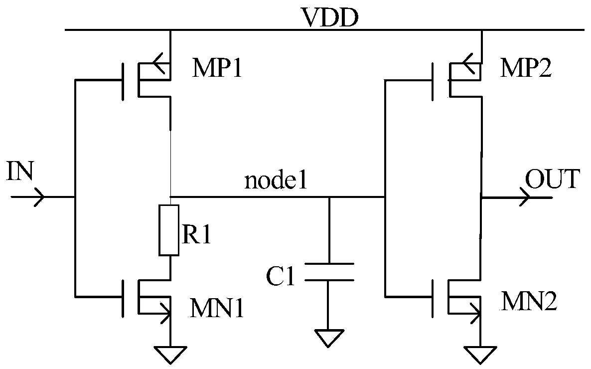
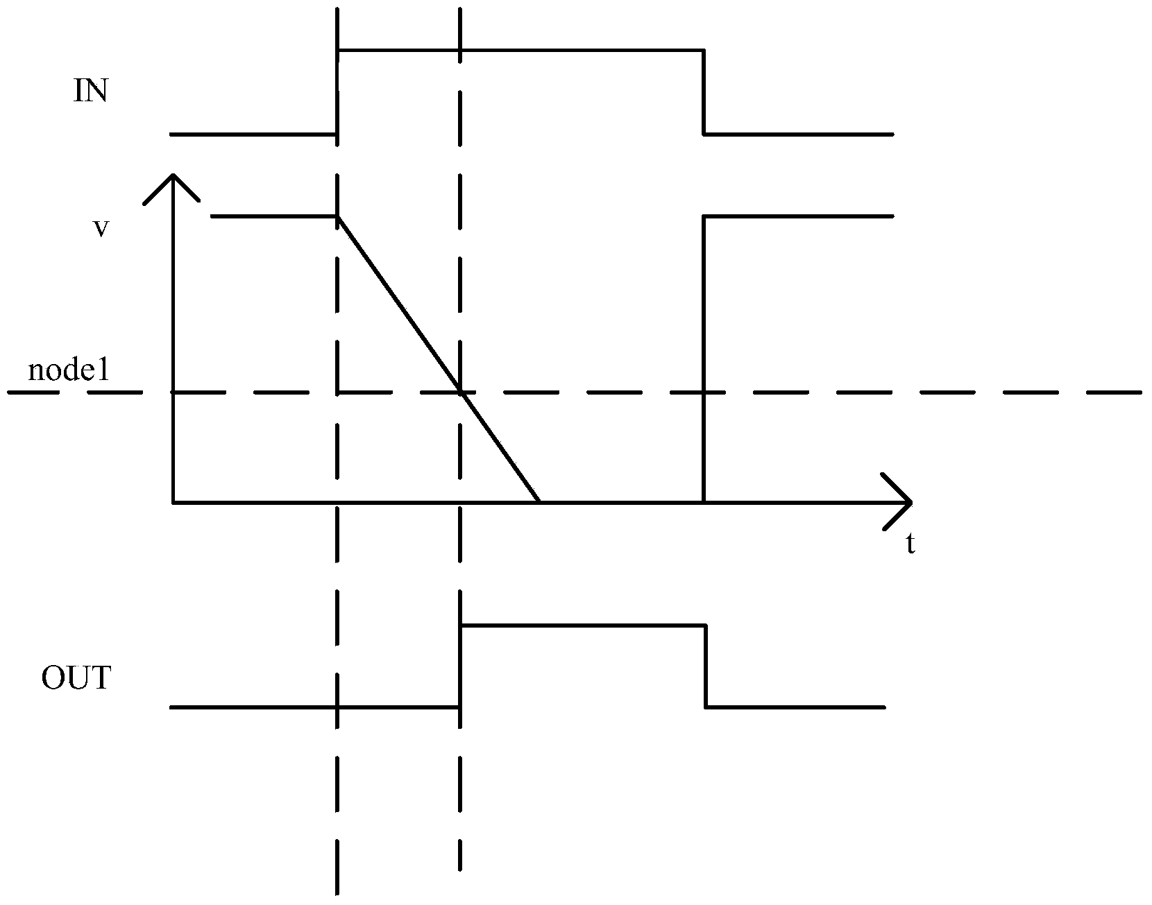
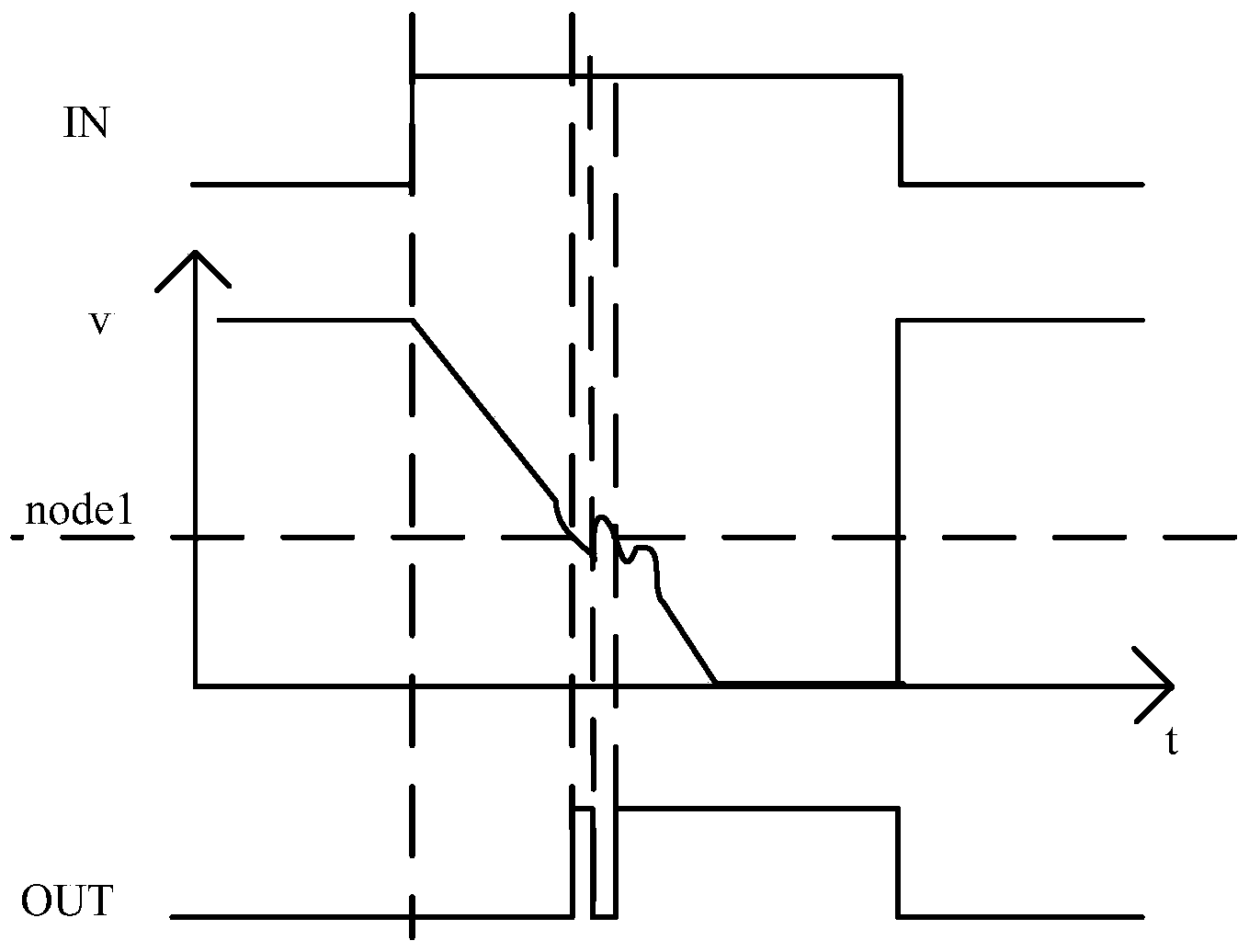
[0027] Figure 4 It is a schematic diagram of the delay unit circuit of the present invention. As shown in the figure, the delay unit circuit specifically includes: a digital signal input port (IN), a digital signal output port (OUT), a first inverter (101), a second inverter device (102), feedback control module (103), node node1, power supply (VDD), capacitor (C1) and resistor (R1).

[0028] In the embodiment of the present invention, the input stage of the first inverter (101) is connected to the digital signal input port IN, the output stage is connected to the node node1, and both ends of the intermediate stage are connected to the power supply VDD and the ground; the second inverter The input stage of the inve...


PUM


Abstract

The invention relates to a delay unit circuit. The circuit comprises signal input and output ports, first and second phase inverters, a feedback control module, a node 1, a power supply, a capacitor and a resistor. The input stage of the first phase inverter is connected with the signal input port, the output stage is connected with the node, and the two ends of the intermediate stage are respectively connected with the power supply and the ground. The input stage of the second phase inverter is connected with the node, the output stage is connected with the signal output port, and the two ends of the intermediate stage are respectively connected with the power supply and the ground. The input stage of the feedback control module is connected with the signal input port, the output stage is connected with a signal output end, and the two ends of the intermediate stage are respectively connected with the node and the ground. The capacitor is connected between the node and the ground or between the node and the power supply. After an input-end signal changes from low to high, the signal is pulled down through the first phase inverter, the capacitor discharges electricity to the ground through the resistor to enable the node level to gradually change from high to low, output of an output-end signal is delayed, and until the node voltage is lower than the flip level, the level of the signal output end is immediately flipped to change from low to high, and the feedback module is switched on and quickly pulls down the node level.

Description

technical field [0001] The invention belongs to the field of integrated circuit design, and in particular relates to a delay unit circuit. Background technique [0002] Delay unit circuits are widely used in various integrated circuits. The delay unit can effectively control the transient overvoltage and voltage mutation in the circuit, buffer the circuit, and protect the safe operation of the device. Some short-time delay units do not use digital clock timing, but use resistors and capacitors to form delays. Because resistors and capacitors are susceptible to noise interference, the output is abnormal. [0003] For example figure 1 It is a delay unit circuit in the prior art. The first inverter includes a first PMOS transistor (MP1) and a first NMOS transistor (MN1), hereinafter referred to as MP1 and MN1, and the second inverter includes a second PMOS transistor (MP2) and a second NMOS transistor (MN2). Hereinafter referred to as MP2 and MN2. IN is a digital signal in...

Claims


Application Information

Patent Timeline
IPC IPC(8): H03K19/0175
Inventor 张汉儒尹航王钊
Owner WUXI ZGMICRO ELECTRONICS CO LTD
Why Eureka
Try Eureka