SOC (system on chip) and design method for same

A system-level chip and computing unit technology, applied in the SOC field, can solve problems such as serious losses, high R&D costs or authorization costs, and delays in product launch time

Inactive Publication Date: 2014-03-26
HANGZHOU XINXUN TECH CO LTD
View PDF4 Cites 4 Cited by
  • Summary
  • Abstract
  • Description
  • Claims
  • Application Information

AI Technical Summary

Problems solved by technology

In the process of changing the tape-out process, the upgrade of digital logic part IP usually rarely brings cost increase and potential risk, but analog unit IP usually needs to be redesigned or authorized, which often leads to the research and development costs or authorization of these analog unit IP The cost is extremely high; and the upgrade and re-spin of the chip will delay the time to market of the product. Once a problem occurs, the loss will be extremely serious

Method used


Image

  • SOC (system on chip) and design method for same
  • SOC (system on chip) and design method for same
  • SOC (system on chip) and design method for same

Examples


no. 1 example

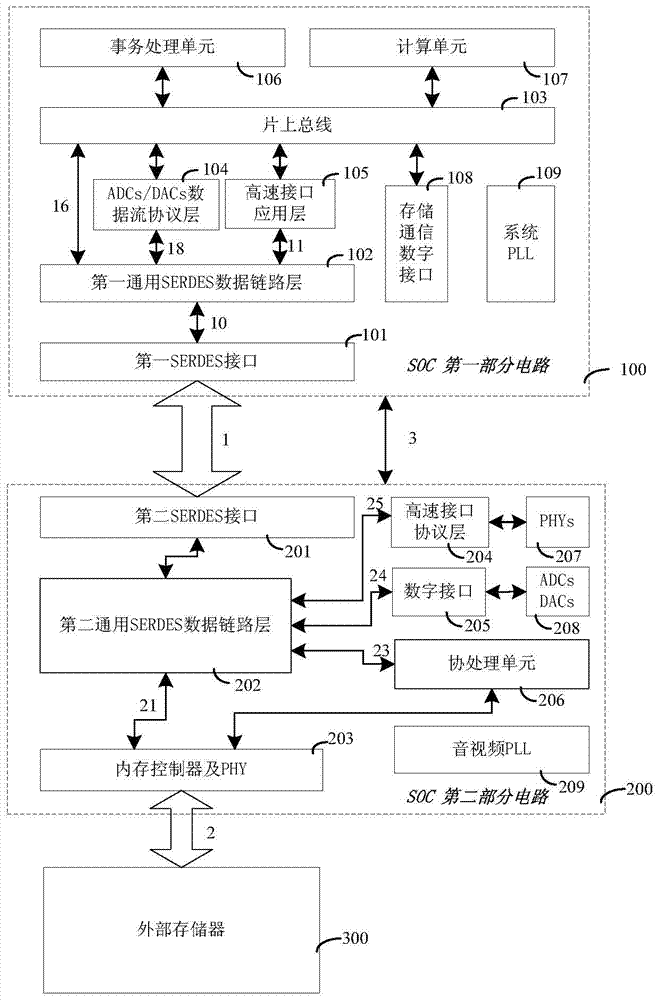
[0089] refer to figure 1 , the system-on-a-chip (or system-on-chip device) of the first embodiment is divided into two parts: the first part of the circuit 100 and the second part of the circuit 200, the two are arranged in different layouts, bare chips, chips or programmable devices and are connected to each other through the SERDES interface, and the data interaction between the two follows the relevant SERDES technical specifications. Among them, the first part of the circuit 100 mainly includes a general digital part, such as one or more SOC digital parts; the second part of the circuit 200 mainly includes a SOC high-speed interface and an analog part, such as one or more SOC analog parts.

[0090] As a preferred embodiment, the first part of the circuit 100 and the second part of the circuit 200 share the same external memory 300 . The external memory 300 can be various suitable volatile memories, such as DDR1 / 2 / 3, LPDDR and so on.

[0091] Further, the first part of th...

no. 2 example

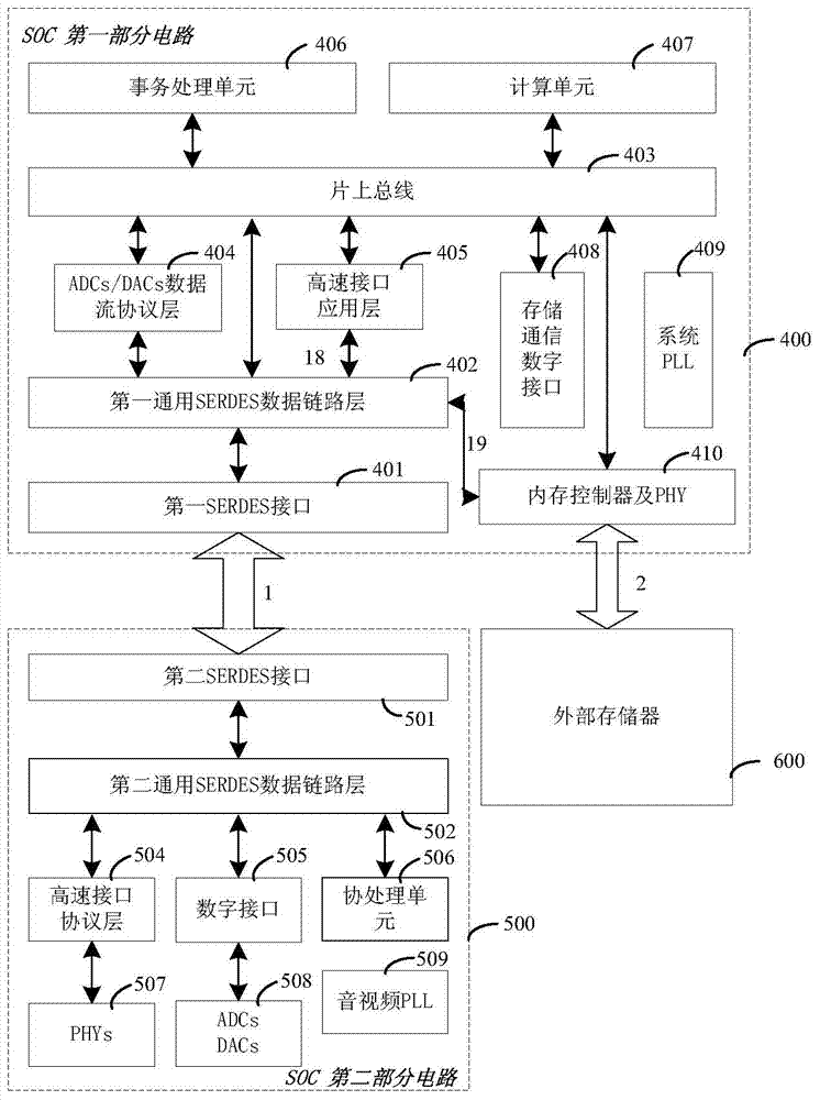
[0115] refer to figure 2 , figure 2 Shows the structural block diagram of the system-on-a-chip or device of the second embodiment, similar to the first embodiment, it is divided into two parts: the first part of the circuit 400 and the second part of the circuit 500, the two are arranged in different layouts, On the bare chip, chip or programmable device, and connected to each other through the SERDES interface, the data interaction between the two follows the relevant SERDES technical specifications. Among them, the first part of the circuit 400 mainly includes a general digital part, such as one or more SOC digital parts; the second part of the circuit 500 mainly includes a SOC high-speed interface and an analog part, such as one or more SOC analog parts.

[0116] As a preferred embodiment, the first part of the circuit 400 and the second part of the circuit 500 share the same external memory 600 . The external memory 600 can be various volatile memories, such as DDR1 / 2 / ...

no. 3 example

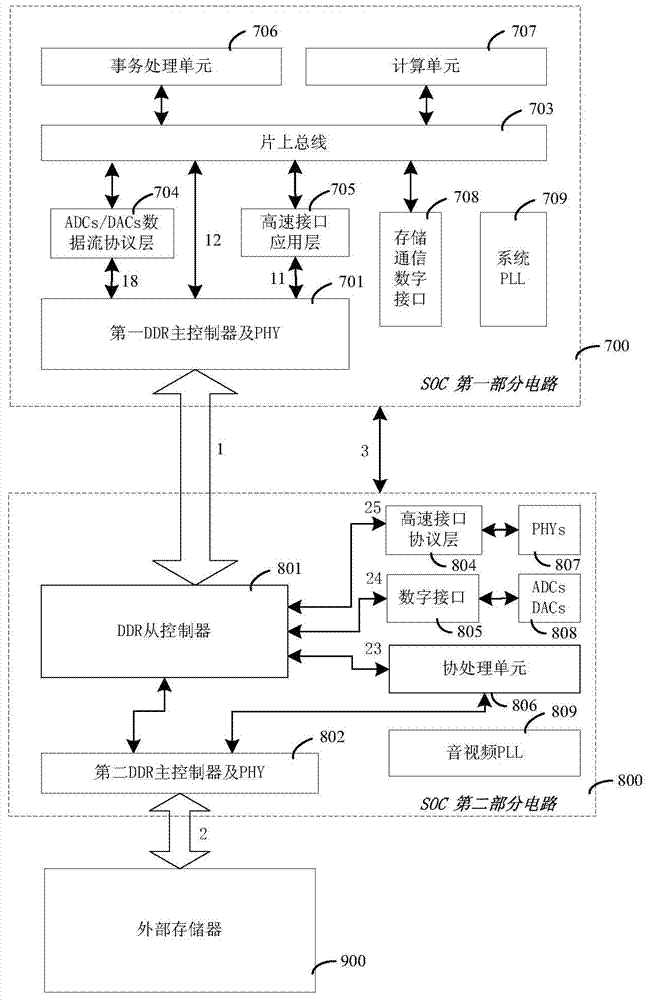
[0125] refer to image 3 , image 3Shows a structural block diagram of the system-on-a-chip or device of the third embodiment, similar to the first and second embodiments, it is divided into two parts: a first part of the circuit 700 and a second part of the circuit 800, the two are arranged in different On the layout, bare chip, chip or programmable device, and are connected to each other through the DDR interface, the data interaction between the two follows the relevant DDR technical specifications. Among them, the first part of the circuit 700 mainly includes a general digital part, such as one or more SOC digital parts; the second part of the circuit 800 mainly includes a SOC high-speed interface and an analog part, such as one or more SOC analog parts.

[0126] As a preferred embodiment, the first part of the circuit 700 and the second part of the circuit 800 share the same external memory 900 . The external memory 900 can be various volatile memories, such as DDR1 / 2 / 3...


PUM


Abstract

The invention provides an SOC (system on chip) and a design method for the same. The SOC comprises a first circuit part and a second circuit part, wherein the first circuit part comprises one or more SOC digital parts; the second circuit part comprises one or more SOC analogue parts; the first and second circuit parts are arranged on different layouts, bare chips, chips or programmable devices, and are connected through a communication interface. According to the SOC and the design method for the same, the design cost of the SOC in a process node upgrading process is greatly lowered, the time-to-market of a product is shortened, and tape-out risks are reduced.

Description

technical field [0001] The invention relates to SOC technology, in particular to a system-level chip and a design method thereof. Background technique [0002] The existing system-on-chip (SOC, System on Chip) design method usually integrates various digital logic IPs and various analog unit IPs on a single chip to maximize the degree of integration. Among them, digital logic IP can include various transaction processing units such as central processing unit (CPU), digital signal processor (DSP), counter (TIMER), watchdog (WATCHDOG), graphics, video, audio, encryption and decryption, etc. A variety of computing units, SDMMC, Universal Asynchronous Receiver Transmitter (UART), Serial Peripheral Interface (SPI) and other digital interfaces, Universal Serial Bus (USB), PCIe, SATA, HDMI and other high-speed serial interfaces The protocol layer and the on-chip bus connecting various devices, but not limited to this; the analog unit IP can include analog-to-digital converter (ADC...

Claims


Application Information

Patent Timeline
Patent Type & Authority Applications(China)
IPC IPC(8): G06F15/78
Inventor 张华胡红旗
Owner HANGZHOU XINXUN TECH CO LTD
Why Eureka
Try Eureka