Method and system for controlling chip die bonder

A control method and technology of a die bonding machine, which are applied in the manufacturing of semiconductor/solid-state devices, electrical components, circuits, etc., can solve the problems such as the positioning accuracy not reaching the preset index, the leakage of multiple chip positions, and the inability to identify all of them. , to achieve good positioning effect, reduce the amount of calculation, and avoid the effect of misjudgment of classification

Inactive Publication Date: 2014-03-26
WUHAN INSTITUTE OF TECHNOLOGY
View PDF4 Cites 4 Cited by
  • Summary
  • Abstract
  • Description
  • Claims
  • Application Information

AI Technical Summary

Problems solved by technology

[0003] However, due to the diversity and flexibility of operating circuit boards, the applicability of the three-dimensional die-bonding positioning platform with fixed XYZ coordinates is very poor, and the mechanical screw has corresponding wear after repeated positioning, resulting in positioning accuracy that is not as expected. set indicators
At present, most die bonder systems have poor repeatability and low assembly or operation accuracy during assembly or operation. Many systems still require semi-automatic assembly with human participation and cannot be fully autonomously assembled or operated.
[0004] The existing vision-guided die-bonding machines often have missing operations of position targets during multi-target recognition (that is, multiple chip positions cannot be fully recognized, resulting in abnormal die bonding), and multi-target chip position recognition on complex circuit boards. There is no corresponding solution for positioning
In addition, the calibration of the internal and external parameters of the visual camera is usually carried out using calibration blocks. The results of such calibration often depend on the accuracy of human calibration, so the positioning effect of the system is often poor, and the movement of the mechanical platform appears to be jittery and the overall deviation of the positioning position. shift

Method used


Image

  • Method and system for controlling chip die bonder
  • Method and system for controlling chip die bonder
  • Method and system for controlling chip die bonder

Examples


Embodiment Construction

[0032] The present invention will be further described below in conjunction with specific examples.

[0033] A method for controlling a chip bonder, comprising the following steps:

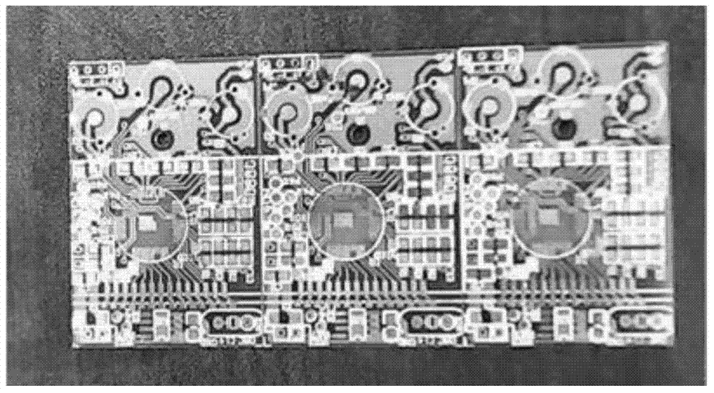
[0034] Step 1. Obtain the image of the motion platform, which contains wafer information; in this embodiment, as figure 1 shown;

[0035] Step 2. Determine the positional relationship between the wafer on the motion platform and the object to be operated according to the image:

[0036] 2.1. Preprocessing the acquired image of the motion platform; preprocessing includes grayscale processing and binarization processing of the image;

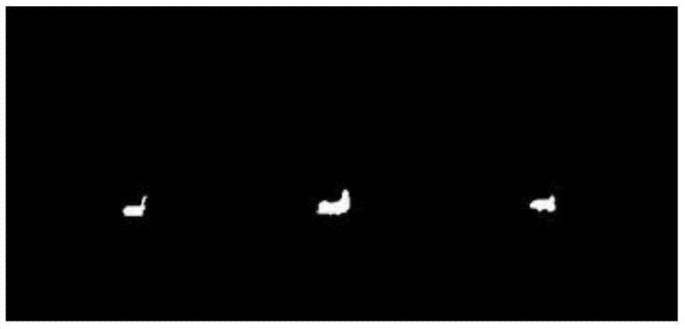
[0037] 2.2, use the edge detection algorithm (canny edge operator is selected to calculate in this embodiment) to the preprocessed image to obtain the edge image; in this embodiment, for example figure 2 shown;

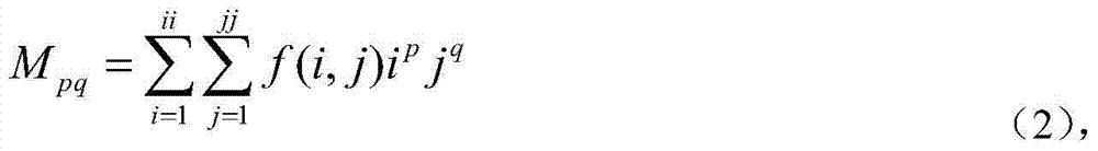
[0038] 2.3. Extract moment invariant features from edge images;

[0039] 2.4. According to the invariant moment characteristics, the three-dimensional ...


PUM


Abstract

The invention provides a method and a system for controlling a chip die bonder. The method comprises the steps of: acquiring the image of a motion platform, and the image includes the information of a wafer; determining the position relationship between the wafer on the motion platform and an operated object according to the image; controlling the movement of an end effector according to the acquired position relationship, so that the wafer on the motion platform moves to a target position; controlling the end effector for die bond. The method and the system control the die bonder in a vision-guided mode; therefore, the positioning effect is good, and the problems of the jitter of mechanical platform motion and the overall deviation of the positioning location can be resolved.

Description

technical field [0001] The invention belongs to the field of semiconductor package control, and in particular relates to a control method and a control system of a chip bonder. Background technique [0002] The structure of the three-dimensional die-bonding platform is composed of the X-axis motion system, the Y-axis motion system, the Z-axis motion system and the terminal die-bonding valve. The three-dimensional coordinates of the fixed position are given, and the manipulator performs repeated positioning of the circuit board chip position, and then controls the end-fixing valve. Crystal valve for chip bonding. [0003] However, due to the diversity and flexibility of operating circuit boards, the applicability of the three-dimensional die-bonding positioning platform with fixed XYZ coordinates is very poor, and the mechanical screw is worn after repeated positioning, resulting in positioning accuracy that cannot reach the expected set indicators. At present, most die bon...

Claims


Application Information

Patent Timeline
Patent Type & Authority Applications(China)
IPC IPC(8): H01L21/68
CPCH01L21/68
Inventor 曾祥进黄紫青王海晖李晓林蔡敦波鲁统伟
Owner WUHAN INSTITUTE OF TECHNOLOGY
Why Eureka
Try Eureka