Method of manufacturing electronic device, electronic apparatus, and mobile apparatus

A technology of electronic devices and manufacturing methods, applied in the manufacture/assembly of piezoelectric/electrostrictive devices, electric solid devices, electrical components, etc.

Inactive Publication Date: 2014-03-26
SEIKO EPSON CORP
View PDF6 Cites 9 Cited by
  • Summary
  • Abstract
  • Description
  • Claims
  • Application Information

AI Technical Summary

Problems solved by technology

[0008] However, in recent years, containers have been increasingly miniaturized. Even as disclosed in Patent Document 1, the structure of the cover body is inclined in such a way that the thickness increases from the edge toward the center of the cover body. Since the thickness of the cover body itself is only 0.1 mm or so, there is still a problem that it is difficult to avoid cracks in the container body due to thermal stress (residual stress) generated during welding

Method used


Image

  • Method of manufacturing electronic device, electronic apparatus, and mobile apparatus
  • Method of manufacturing electronic device, electronic apparatus, and mobile apparatus
  • Method of manufacturing electronic device, electronic apparatus, and mobile apparatus

Examples


Embodiment Construction

[0037] Hereinafter, embodiments of the present invention will be described in detail with reference to the drawings.

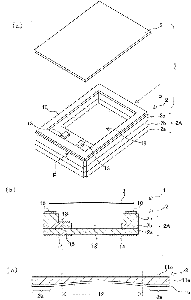
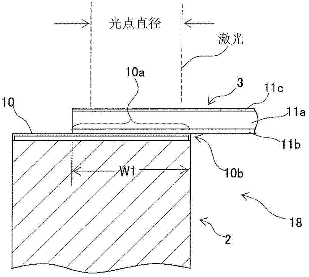
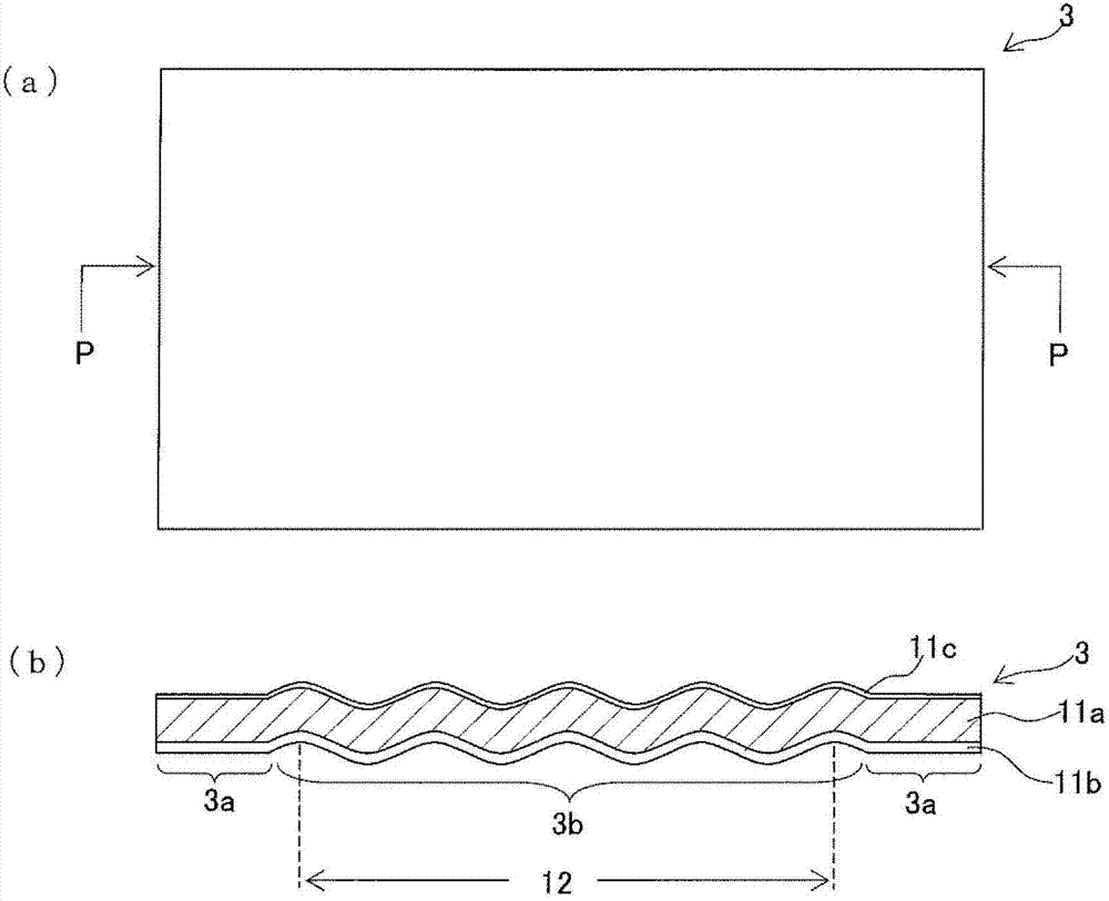
[0038] figure 1 (a) is an exploded perspective view of one embodiment of the electronic device container 1 of the present invention, (b) of the figure is a PP sectional view of (a), and (c) of the figure is an enlarged sectional view of the lid body 3 .

[0039] The container 1 for accommodating electronic components includes: a base substrate (container body) 2 made of ceramics having a concave portion on which the electronic component can be mounted; Cover 3.

[0040] The outline of the manufacturing method of the container 1 for electronic devices of this invention is as follows. That is, this manufacturing method is a method of manufacturing an electronic device container 1 provided with a base substrate 2 having an insulating substrate 2A made of ceramics and a metal lid 3, and the manufacturing method has the following steps: : Prepare the base subst...


PUM


Abstract

The invention provides a method of manufacturing an electronic device, an electronic apparatus, and a mobile apparatus. No cracks can be generated on the ceramic material of a base substrate when a lid is joined to the sealing part of the base substrate. The method of manufacturing the electronic device including an electronic element, a base substrate, and a lid member, includes joining the lid member to the sealing part by application of an energy beam so that a plate thickness of the lid member may be larger in a part joined to the sealing part than in a part located inside of the part in a plan view along the thickness direction.

Description

technical field [0001] The present invention relates to a method of manufacturing an electronic device that realizes an improved method of welding a container body and a lid, an electronic device using the method, and a mobile device. Background technique [0002] As a structure for hermetically sealing electronic components in the container, electronic components are arranged in a ceramic container body that is open on one side, and electrical conduction between the electronic components and the wiring on the container body side is achieved using conductive members, and then the container body is used. A method of seam-welding (resistance welding) the sealing portion formed at the periphery of the opening and a metal cover to seal, or a method of joining them by melting them with a laser or an electron beam, or the like. [0003] In Patent Document 1, a piezoelectric device manufactured using seam welding is disclosed. The piezoelectric device has a container for electroni...

Claims


Application Information

Patent Timeline
Patent Type & Authority Applications(China)
IPC IPC(8): H01L23/02
CPCH03H9/1057H03H9/1071H01L41/23G01C19/5628H03H9/1021H03H9/10H01L2924/16195Y10T29/42B23K2101/36H10N30/02B23K1/0016B23K1/005
Inventor 宫坂英男
Owner SEIKO EPSON CORP
Why Eureka
Try Eureka