Vertical microelectronic component and corresponding manufacturing method

A technology of microelectronic components and areas, applied in the direction of electrical components, semiconductor/solid-state device manufacturing, electric solid-state devices, etc., to achieve the effects of small resistance, high power density, and small area consumption

Inactive Publication Date: 2018-11-16
ROBERT BOSCH GMBH
View PDF6 Cites 0 Cited by
  • Summary
  • Abstract
  • Description
  • Claims
  • Application Information

AI Technical Summary

Problems solved by technology

This problem is particularly important for high voltage classes above 600 V, since in side elements a high compressive strength can only be achieved by increasing the distance between the gate connection and the discharge connection

Method used


Image

  • Vertical microelectronic component and corresponding manufacturing method
  • Vertical microelectronic component and corresponding manufacturing method
  • Vertical microelectronic component and corresponding manufacturing method

Examples


Embodiment Construction

[0020] In the figures, identical reference numbers designate identical or functionally identical elements.

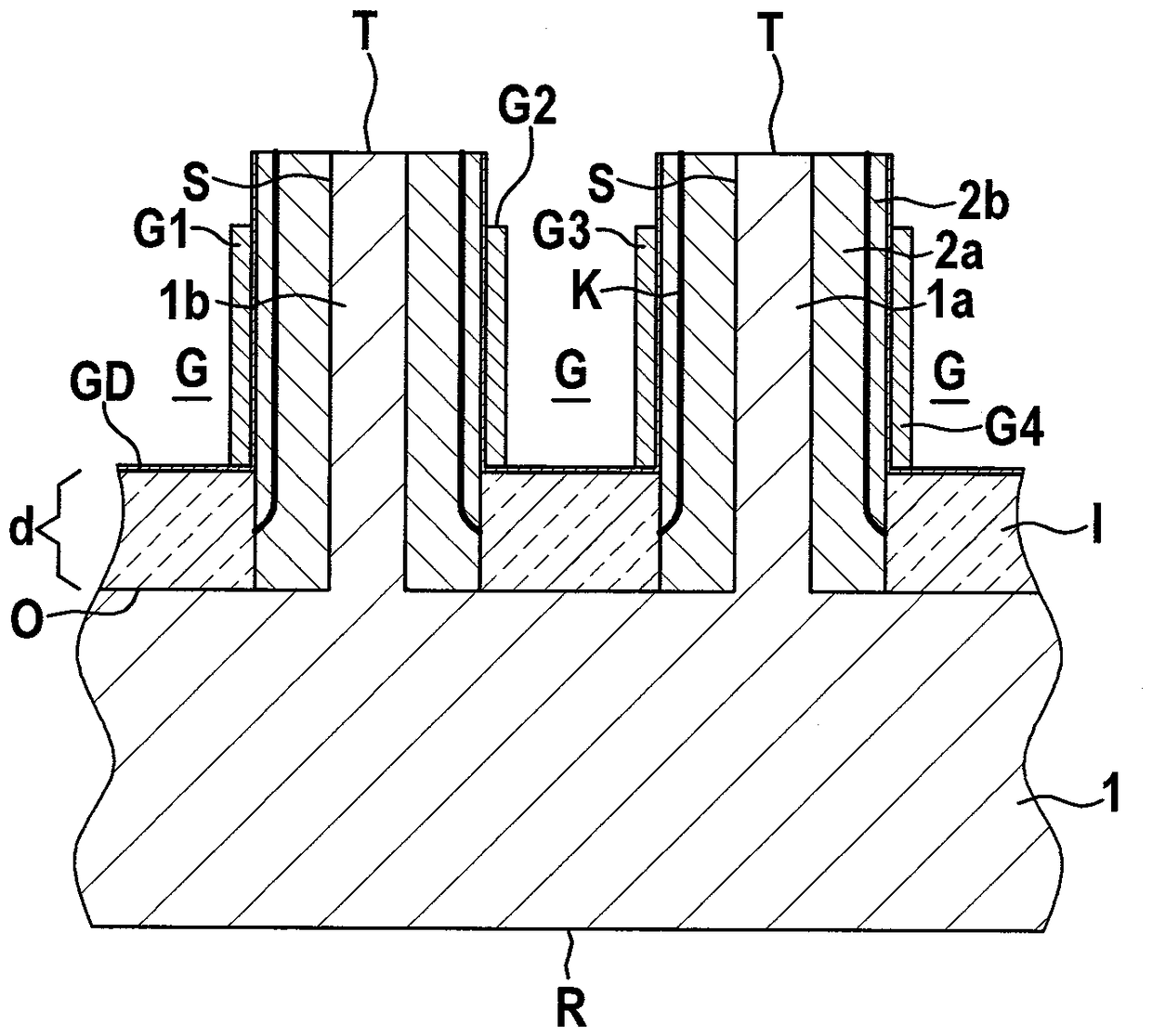
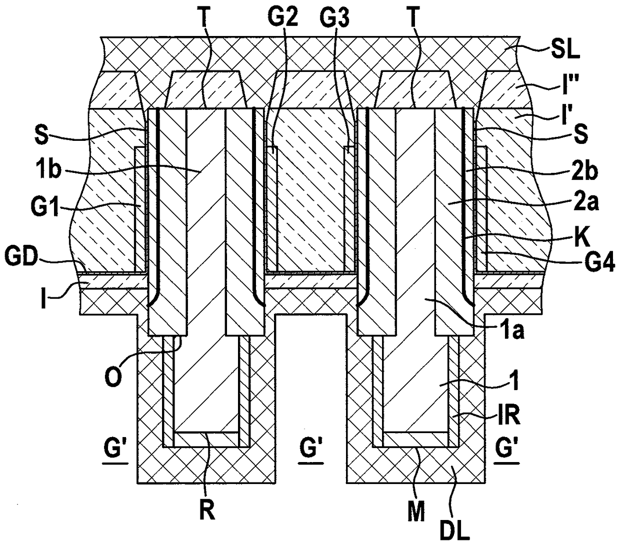
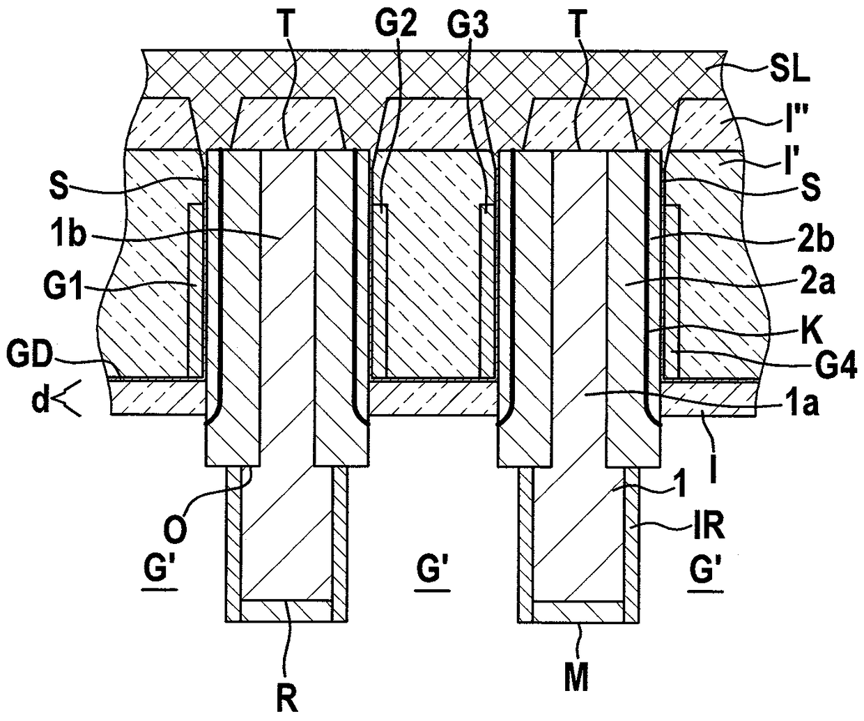
[0021] Figure 1a )-o) are schematic cross-sectional views for explaining a vertical microelectronic component according to an embodiment of the invention and the corresponding manufacturing method.

[0022] exist Figure 1a ), reference numeral 1 denotes a silicon-semiconductor base having a front side O and a backside R. On the front side O of the silicon-semiconductor base 1 a large number of fins 1a, 1b are formed by means of a trench etching process, between which there are recesses G in the silicon-semiconductor base. In this example, the etched recess G is selected such that it lies perpendicular to the (111) crystal plane in the silicon-semiconductor substrate 1 . The side walls of the fins 1a, 1b are denoted by reference S, and the upper faces thereof by T. The structure of the fins 1a, 1b can be one-dimensional (for example linear), but also two-dimensional ...


PUM


Abstract

The invention realizes a vertical microelectronic element and a corresponding manufacturing method. The vertical microelectronic element comprises a structure of a semiconductor base (1; 1''') and a plurality of fins (1a, 1b) formed on the front side (O) of the semiconductor base (1; 1'''), the The semiconductor base has a front side (O) and a rear side (R), and the fins have respective side walls (S) and respective upper sides (T) and are separated from each other by recesses (G). Each fin (1a, 1b) comprises at least one GaN / AlGaN-heterolayer region (2a, 2b) and at least one gate interface region (G1-G4), said GaN / AlGaN-heterolayer region formed on the sidewall (S) and has an embedded channel region (K) extending essentially parallel to the sidewall (S), the gate interface region above the GaN / AlGaN-heterolayer region (2a, 2b) with the associated The channel region (K) in the recess (G) is arranged electrically insulatingly on the side wall (S). A common source interface region (SL) is arranged above the fins (1a, 1b) and is connected to respective first ends of the channel regions (K) near the upper side (T) of the fins (1a, 1b). A common drain interface region (DL) is arranged above the rear side (R) and is connected to the respective second ends of the channel region (K) near the front side (O) of the semiconductor substrate (1, 1''').

Description

technical field [0001] The invention relates to a vertical microelectronic component and a corresponding manufacturing method. Background technique [0002] HEMT-transistors (High-Electron-Mobility Transistor=Transistor mit hoherElektronenbeweglichkeit) are special structures of field-effect transistors which are especially suitable for use at high frequencies due to their low component capacitance. Starting from the structure, HEMT transistors are formed from layers of different semiconductor materials with band gaps of different sizes (so-called heterolayer structures), for which the material system GaN / AlGaN is used, for example. If the two materials are deposited on top of each other, a two-dimensional electron gas is formed on both sides of the GaN at the interface of the materials, which can be used as a conductive channel because the electron mobility is very large in it. High. [0003] Conventional HEMT transistors with the material system GaN / AlGaN are produced in...

Claims


Application Information

Patent Timeline
Patent Type & Authority Patents(China)
IPC IPC(8): H01L29/778H01L29/06H01L21/335
CPCH01L29/42372H01L29/66462H01L29/7789H01L29/2003H01L29/1608H01L29/7855H01L29/7788H01L21/18H01L29/778H01L2924/1033
Inventor C.舍林W.达夫斯
Owner ROBERT BOSCH GMBH
Why Eureka
Try Eureka