Method for forming breakage holes in printed circuit board

A technology for printed circuit boards and manufacturing methods, applied in the direction of electrical connection formation of printed components, etc., can solve the problems of poor plating resistance and high ink requirements, and achieve the effect of low requirements and low material cost

Active Publication Date: 2014-03-26
GUANGZHOU MEADVILLE ELECTRONICS
View PDF3 Cites 12 Cited by
  • Summary
  • Abstract
  • Description
  • Claims
  • Application Information

AI Technical Summary

Problems solved by technology

[0008] The purpose of the present invention is to propose a method for making broken holes in printed

Method used


Image

  • Method for forming breakage holes in printed circuit board
  • Method for forming breakage holes in printed circuit board
  • Method for forming breakage holes in printed circuit board

Examples


Embodiment Construction

[0035] In the following, the present invention will be further described in conjunction with the drawings and specific embodiments.

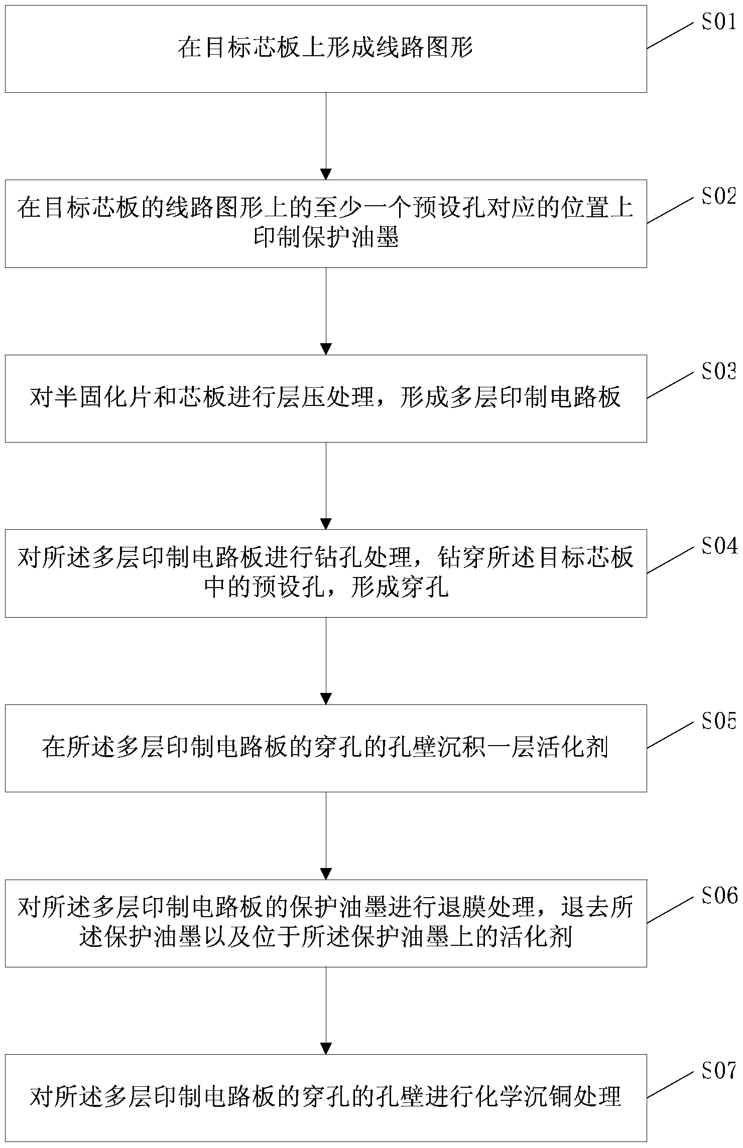
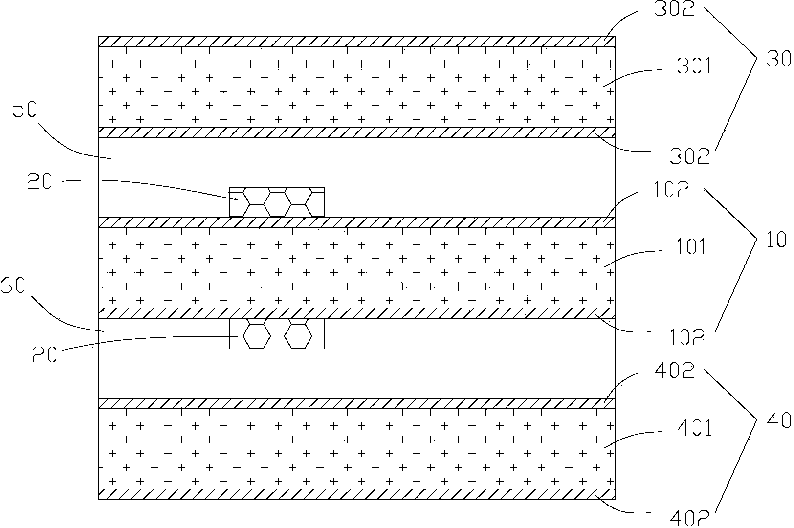
[0036] Such as Figure 1 to Figure 6 Shown, a kind of broken hole manufacture method of printed circuit board, it comprises the following steps:

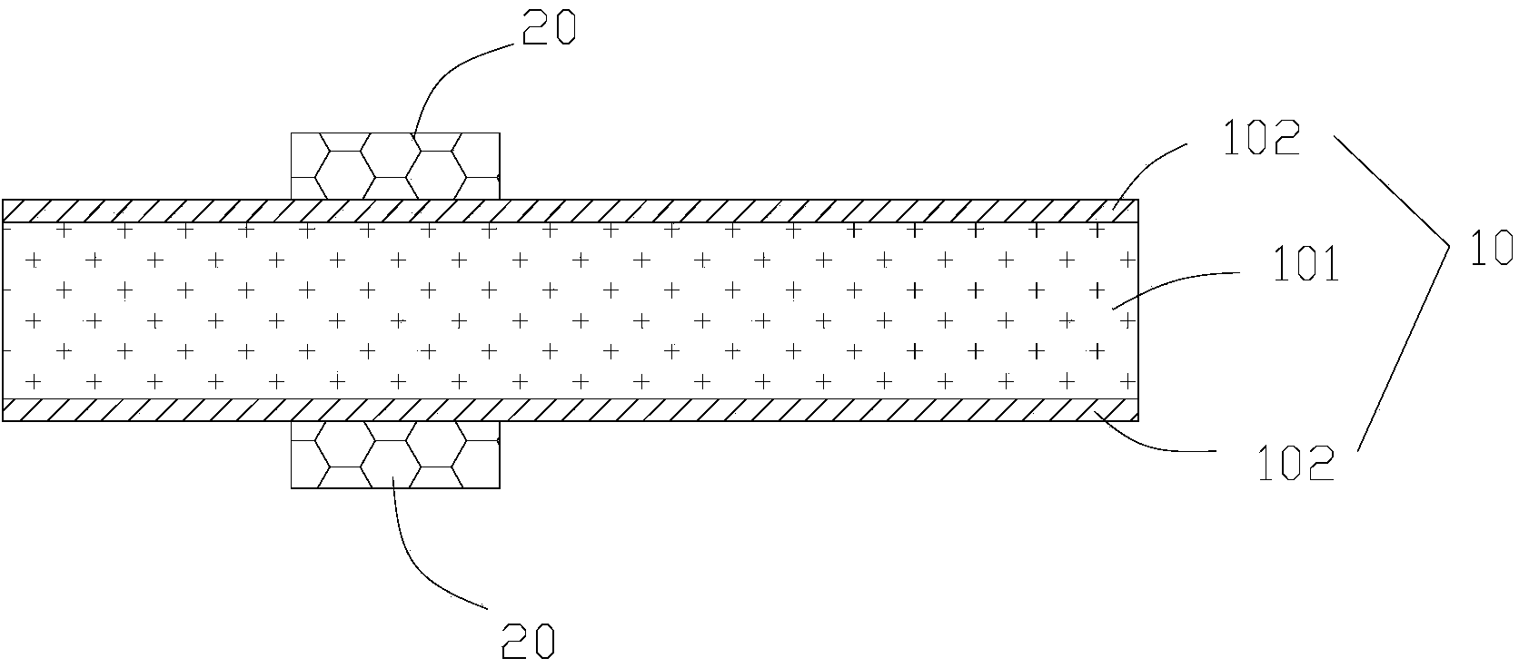
[0037] Step S01, forming a circuit pattern on the double-sided copper foil layer 102 of the target core board 10 through film sticking, exposure, and etching; the target core board 10 includes an insulating layer 101 and a double-sided copper foil on the insulating layer 101 layer 102 , and the circuit pattern is located on the copper foil layer 102 .

[0038] Step S02, printing protective ink 20 on the position corresponding to at least one preset hole on the double-sided circuit pattern of the target core board 10, the radius of the protective ink 20 is larger than the preset hole, wherein the preset The hole is a hole that does not need to transmit electrical signals between layers; the protectiv...


PUM


Abstract

The invention relates to a method for forming breakage holes in a printed circuit board. The method comprises the following steps of printing protective printing ink on a circuit graph of an objective cross-band veneer; performing normal pressing-fit and drilling procedures; and thoroughly peeling the protective printing ink before chemical copper deposition by using an organic solvent so as to prevent hole walls printed with the protective printing ink from being deposited with chemical copper and electroplating copper in a subsequent hole metalizing process. Activating agents absorbed on the surface of the protective printing ink can be removed together with the protective printing ink, and the organic solvent cannot damage resin and activating agents on glass fibers, so that a chemical copper layer serving as an electroplating seed layer is deposited on hole walls of whole perforated holes expect for a cavity; and the chemical copper cannot be deposited on the surface of a material positioned on the cavity because the activating agents are not adhered to the surface of the material, and a conductive layer cannot be formed. The method for forming the breakage holes in the printed circuit board is simple in manufacturing procedure and low in cost; requirements on materials are low; batch production is realized easily; and a plating resisting effect can reach 100%.

Description

[0001] technical field [0002] The invention relates to the field of printed circuit boards, in particular to a method for manufacturing broken holes of printed circuit boards. [0003] Background technique [0004] With the continuous development of communication and network technology, the signal transmission rate is getting higher and higher, and high-frequency circuits are widely used in the design of electronic products. In order to meet the normal transmission of high-frequency signals in the printed circuit board (Printed Circuit Board, PCB), more stringent requirements are put forward for the design and manufacture of the PCB. At present, PCB adopts through holes, buried holes or blind holes for electrical connection, so as to realize the interconnection between layers. Under the existing PCB manufacturing technology, when the plated through hole is used as the transmission medium between layers, the electrical signal passes through the wire of one layer of the PC...

Claims


Application Information

Patent Timeline
IPC IPC(8): H05K3/42
Inventor 王小峰周咏角真司
Owner GUANGZHOU MEADVILLE ELECTRONICS
Why Eureka
Try Eureka