A kind of preparation method of anisotropic silicon quantum dot film
A silicon quantum dot and anisotropic technology, which is applied in the field of preparation of anisotropic silicon quantum dot thin films embedded in an amorphous medium, can solve the problems such as the inability to improve the manufacturing complexity of photovoltaic devices and the limitation of optoelectronic properties. , to achieve the effect of facilitating carrier transport, improving light absorption characteristics, enhancing absorption utilization and high photoelectric conversion efficiency.
- Summary
- Abstract
- Description
- Claims
- Application Information
AI Technical Summary
Problems solved by technology
Method used
Image
Examples
preparation example Construction
[0027] The preparation method of the anisotropic silicon quantum dot thin film of the present invention adopts following scheme, comprises the following steps:
[0028] 1) Select glass and / or silicon wafer as the substrate and pre-treat before coating;
[0029] The thickness of the substrate is 500-520 μm, and it is ultrasonically cleaned for 15-20 minutes by surfactant cocoic acid monoethanolamide (CMEA) or cocoic acid diethanolamide, (flowing) deionized water, acetone, and absolute ethanol in sequence.
[0030] 2) Using Ar gas as the sputtering gas, under the condition of applying a negative bias voltage of 80V to the substrate, use RF and DC power sources to sputter silicon-germanium alloy targets and carbon targets respectively;
[0031] The film deposition and characterization adopt the magnetron sputtering equipment produced by German SPECS company and the supporting online detection device; the size specification of the silicon-germanium alloy target and the carbon targ...
Embodiment 1
[0042]Glass is selected as the substrate and pre-treated before coating. The thickness of the substrate is 500 μm, which is passed through the surfactant cocoic acid monoethanolamide (CMEA) or commercial white cat detergent, (flowing) deionized water, acetone, and absolute ethanol in sequence. Each was ultrasonically cleaned for 15 min.
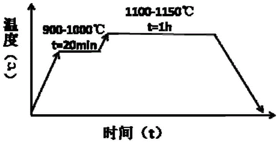
[0043] Using argon as the sputtering gas, magnetron co-sputtering is performed on the silicon-germanium alloy target and the carbon target, and an amorphous silicon-germanium carbide film with an atomic ratio of silicon, germanium and carbon of about 7:1:2 is deposited on the glass substrate. Among them, the silicon-germanium alloy target uses a 100W RF power supply, the carbon target uses a 100W DC power supply, and the substrate bias voltage is 80V; the sputtering Ar gas flow rate is 4 sccm; the deposition time is about 2 hours, and the film thickness is about 150nm. The sample was annealed in stages under nitrogen gas: first, the temperatu...
Embodiment 2
[0047] Silicon wafers were selected as the substrate and pre-treated before coating. The thickness of the substrate was 520 μm, and it was ultrasonically cleaned with surfactant coconut acid diethanolamide, (flowing) deionized water, acetone, and absolute ethanol in sequence for 20 minutes.
[0048] Using argon as the sputtering gas, magnetron co-sputtering is carried out on the silicon-germanium alloy target and the carbon target, and an amorphous silicon-germanium carbide film with an atomic ratio of silicon, germanium and carbon of about 6.5:1.5:2 is deposited on the silicon substrate. . Among them, the silicon-germanium alloy target uses a 120W RF power supply; the carbon target uses a 130W DC power supply; the substrate bias voltage is 80V; the sputtering Ar gas flow rate is 4 sccm; the deposition time is about 2.2h, and the film thickness is about 150nm. The sample was annealed in stages under nitrogen gas: first, the temperature was raised from room temperature to 1000°...
PUM
| Property | Measurement | Unit |
|---|---|---|
| thickness | aaaaa | aaaaa |
| band gap | aaaaa | aaaaa |
| band gap | aaaaa | aaaaa |
Abstract
Description
Claims
Application Information
