Heterojunction solar cell and interfacing processing method and preparing technology thereof

A technology of solar cells and manufacturing processes, applied in circuits, photovoltaic power generation, electrical components, etc.

Inactive Publication Date: 2014-04-30
TRINA SOLAR CO LTD
View PDF3 Cites 10 Cited by
  • Summary
  • Abstract
  • Description
  • Claims
  • Application Information

AI Technical Summary

Problems solved by technology

However, in addition to the dangling bond-related defects in the separation and transport of photogenerated carriers, the strength of the built-in potential field at the interface is directly related to whether the carriers at the interface can be smoothly "swept" into the emitter. However, it is finally collected by electrodes, the interface treatment of thin film / crystalline silicon and the modulation of internal potential field are the difficulties in the research and development of heterojunction cells.

Method used


Image

  • Heterojunction solar cell and interfacing processing method and preparing technology thereof
  • Heterojunction solar cell and interfacing processing method and preparing technology thereof

Examples


Embodiment Construction

[0021] In order to make the content of the present invention more clearly understood, the present invention will be further described in detail below based on specific embodiments and in conjunction with the accompanying drawings.

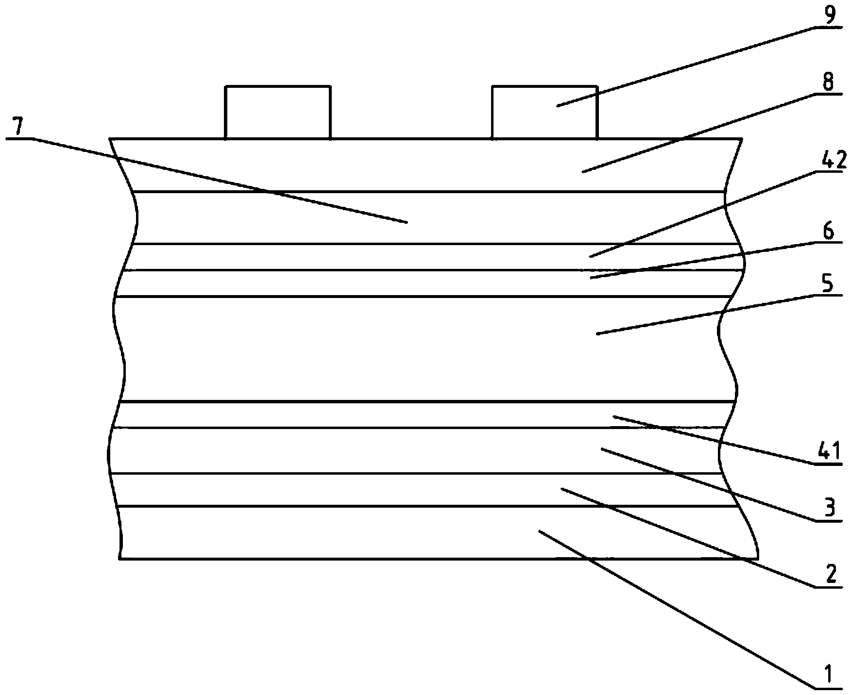
[0022] A preparation process for a heterojunction solar cell, the steps of which are as follows:

[0023] 1) A crystalline silicon wafer is used as the crystalline silicon substrate 5, and its surface is cleaned; the thickness of the crystalline silicon wafer is 200 μm, and the resistivity is 2-5 Ω·cm; the cleaning can be conventional RCA cleaning.

[0024] 2) Next, the front surface of the crystalline silicon substrate 5 is treated with the interface treatment method of the heterojunction solar cell to prepare the heavily doped layer 6; the interface treatment method of the heterojunction solar cell is: in the heterojunction solar cell In the preparation process, the front surface of the crystalline silicon wafer is highly doped by ion implantatio...


PUM

PropertyMeasurementUnit
thicknessaaaaaaaaaa
thicknessaaaaaaaaaa
electrical resistivityaaaaaaaaaa

Abstract

The invention discloses a heterojunction solar cell and an interfacing processing method and preparing technology thereof. According to the interface processing method of the heterojunction solar cell, in the preparing technology of the heterojunction solar cell, highly doping processing is conducted on the front surface of a crystalline silicon wafer with the ion implantation technology or the diffusion technology so that a heavy doped layer can be formed on the front surface of the crystalline silicon wafer, and then the Fermi level of the surface of the crystalline silicon water of the heterojunction solar cell is changed and an built-in electric field is enhanced. According to the method, the built-in electric field of the substrate interface of crystalline silicon can be enhanced, separation and conveyance of current carriers on the border of a depletion region can be promoted more effectively, film/crystalline silicon abrupt junction formation is facilitated, the width of a depletion layer on the base region of the crystalline silicone is reduced, light absorption efficiency is improved, recombination losses of the current carriers are reduced, and the voltage characteristic of a heterojunction efficient battery is improved.

Description

technical field [0001] The invention relates to a heterojunction solar cell and its interface treatment method and preparation process, belonging to the technical field of heterojunction solar cells. Background technique [0002] At present, the technical advantage of heterojunction high-efficiency solar cells lies in the high opening voltage characteristics determined by the heterojunction, and the excellent film / crystalline silicon interface directly contributes to the opening voltage performance of heterojunction cells. Traditional interfacial properties mainly refer to the passivation of dangling bonds on the surface of crystalline silicon. However, in addition to the dangling bond-related defects in the separation and transport of photogenerated carriers, the strength of the built-in potential field at the interface is directly related to whether the carriers at the interface can be smoothly "swept" into the emitter. Finally, it is collected by electrodes, the treatmen...

Claims


Application Information

Patent Timeline
Patent Type & Authority Applications(China)
IPC IPC(8): H01L31/18H01L31/072H01L31/0747
CPCY02E10/50H01L31/03529H01L31/0747H01L31/1804Y02E10/547
Inventor 郭万武
Owner TRINA SOLAR CO LTD
Why Eureka
Try Eureka