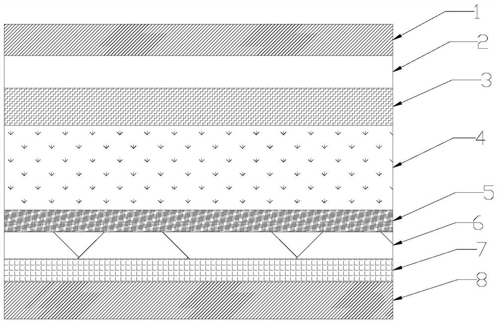
A kind of double-sided cadmium telluride thin-film solar cell and its preparation method
A solar cell and cadmium telluride technology, which is applied in the field of solar cells, can solve the problems that cadmium telluride solar cells cannot generate electricity on both sides, and the absorption layer cannot absorb sunlight from the back, so as to improve Voc and FF and improve performance , The effect of increasing power generation
- Summary
- Abstract
- Description
- Claims
- Application Information
AI Technical Summary
Problems solved by technology
Method used
Image
Examples
Embodiment 1
[0030] A method for preparing a cadmium telluride thin-film solar cell generating electricity on both sides, comprising the following steps:
[0031] (1) Deposit fluorine-doped tin oxide on a glass substrate to form a transparent conductive film layer, and the deposition temperature condition is lower than 400°C;
[0032] (2) Depositing cadmium sulfide on the transparent conductive film layer to form a window layer, the deposition temperature condition is lower than 250°C;
[0033] (3) Depositing cadmium telluride on the window layer to form an absorber layer, the deposition temperature condition is lower than 300°C;
[0034] (4) Depositing cuprous thiocyanate on the absorber layer to form a back contact layer, the deposition temperature condition is lower than 300°C;
[0035] (5) Depositing tungsten-doped indium oxide on the back contact layer to form a back electrode layer, the deposition temperature condition is lower than 300°C;
[0036] (6) Laminate and encapsulate the ...
Embodiment 2
[0039] A method for preparing a cadmium telluride thin-film solar cell generating electricity on both sides, comprising the following steps:
[0040] (1) Deposit fluorine-doped tin oxide on a glass substrate to form a transparent conductive film layer, and the deposition temperature condition is lower than 400°C;
[0041] (2) Depositing cadmium sulfide on the transparent conductive film layer to form a window layer, the deposition temperature condition is lower than 250°C;
[0042] (3) Depositing cadmium telluride on the window layer to form an absorber layer, the deposition temperature condition is lower than 300°C;
[0043] (4) Depositing cuprous thiocyanate on the absorber layer to form a back contact layer, the deposition temperature condition is lower than 300°C;
[0044] (5) Depositing tungsten-doped indium oxide on the back contact layer to form a back electrode layer, the deposition temperature condition is lower than 300°C;
[0045] (6) Laminate and encapsulate the ...
Embodiment 3
[0047] Embodiment 3 (comparative example):
[0048] A method for preparing a cadmium telluride thin film solar cell, comprising the following steps:
[0049] (1) Deposit fluorine-doped tin oxide on a glass substrate to form a transparent conductive film layer, and the deposition temperature condition is lower than 400°C;
[0050] (2) Depositing cadmium sulfide on the transparent conductive film layer to form a window layer, the deposition temperature condition is lower than 250°C;
[0051] (3) Depositing cadmium telluride on the window layer to form an absorber layer, the deposition temperature condition is lower than 300°C;
[0052] (4) Deposit carbon paste on the absorber layer to form a back contact layer, and the deposition temperature condition is lower than 300°C;
[0053] (5) Depositing metallic nickel on the back contact layer to form a back electrode layer, the deposition temperature condition is lower than 300°C;
[0054] (6) Laminate and encapsulate the deposited...
PUM
 Abstract
Description
Claims
Application Information

