

Photovoltaic Apparatus Including Spherical Semiconducting Particles
a photovoltaic apparatus and semiconducting particle technology, applied in the direction of photovoltaic energy generation, electrical apparatus, basic electric elements, etc., can solve the problems of photovoltaic apparatus, high cost of apparatus, complex manufacturing of semiconductor wafers, etc., and achieve the effect of reducing the number of photoelectric conversion elements and efficiently using for generation
- Summary
- Abstract
- Description
- Claims
- Application Information
AI Technical Summary
Benefits of technology
Problems solved by technology
Method used
Image

Examples
Embodiment Construction
[0065]Now referring to the drawings, preferred embodiments of the invention are described below.
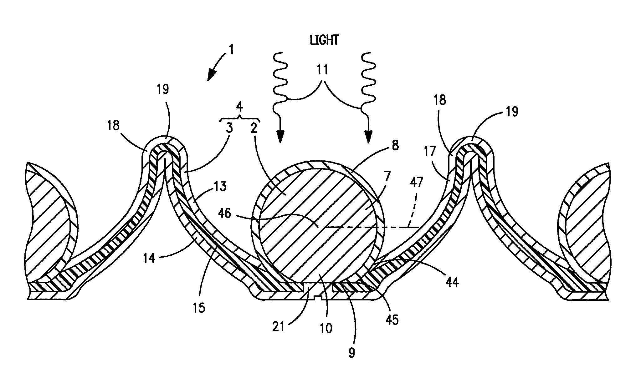
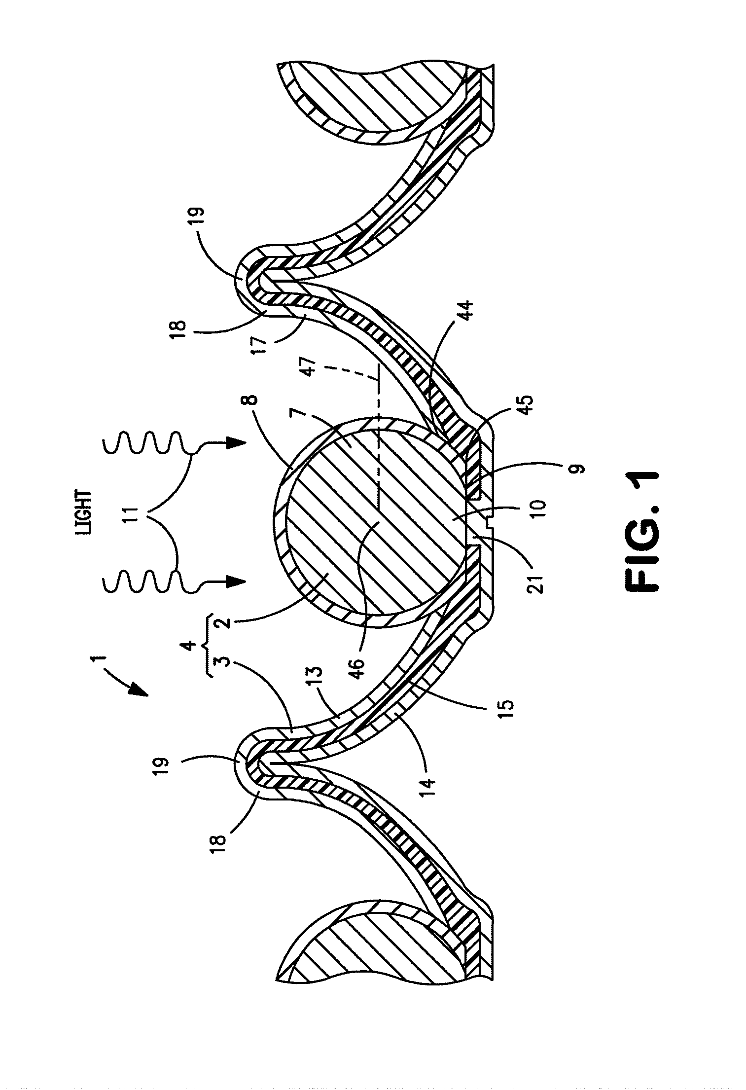
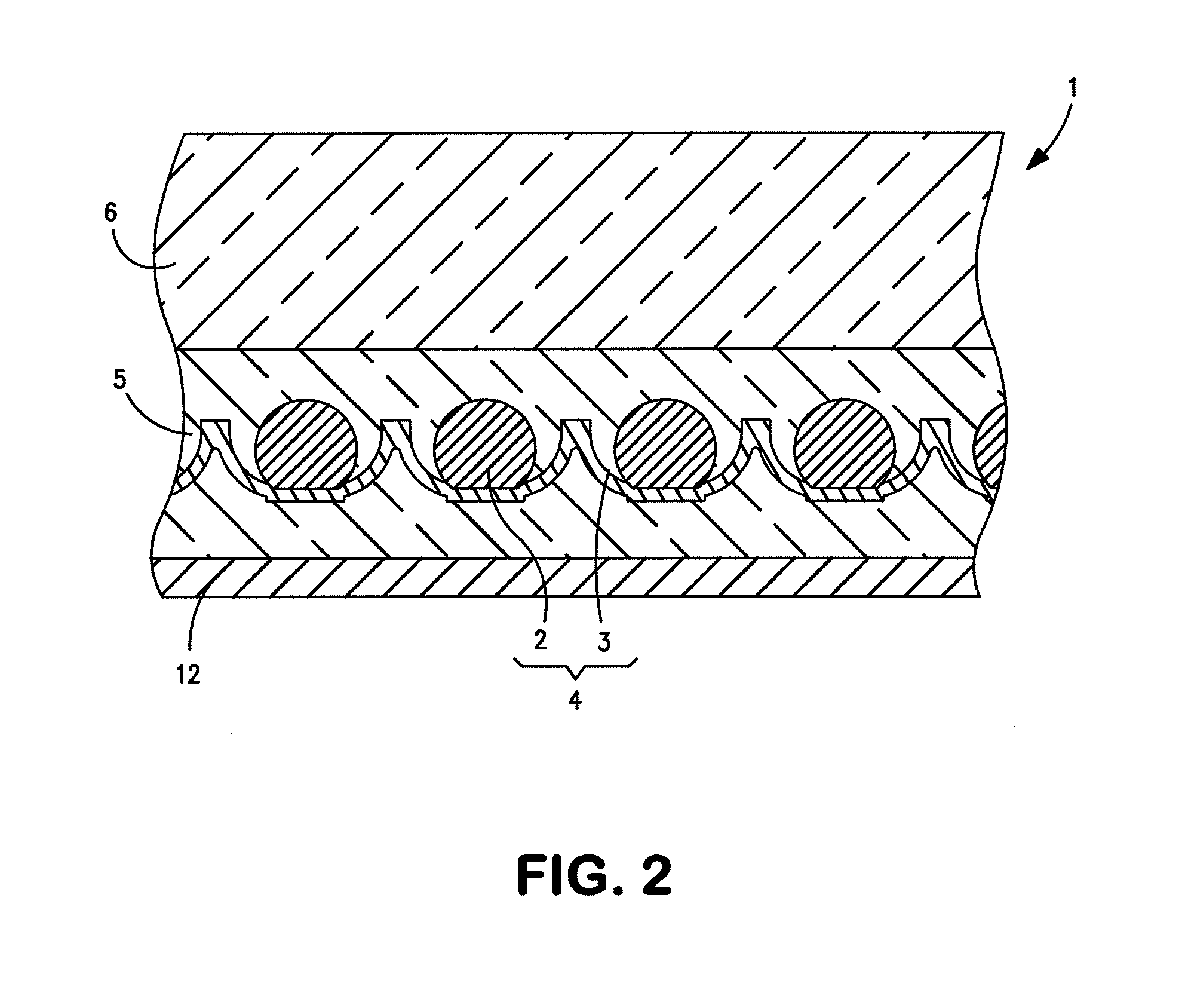
[0066]FIG. 1 is an enlarged sectional view of part of a photovoltaic apparatus 1 according to an embodiment of the present invention. FIG. 2 is a sectional view showing the structure of the photovoltaic apparatus 1. FIG. 3 is an exploded perspective view of the photovoltaic apparatus 1 of FIG. 2. The photovoltaic apparatus 1 has the following basic structure. An assembly 4 of a plurality of generally spherical photoelectric conversion elements 2 and a support 3 that is mounted with the photoelectric conversion elements 2 is buried in a filler layer 5 made of a transparent synthetic resin material such as PVB (poly(vinyl butyral)) or EVA (ethylene vinyl acetate). A transparent protective sheet 6 made of polycarbonate or the like is provided on the light source (e.g., sunlight) side of the filler layer 5 and is fixed to it. A waterproof back sheet 12 is fixed to the surface of the filler la...
PUM
 Abstract
Description
Claims
Application Information