Heterojunction solar cell and manufacturing method thereof

A technology of solar cells and heterojunctions, applied in circuits, photovoltaic power generation, electrical components, etc., can solve the problems of reduced production costs, expensive equipment, and high cost of ion implantation.

Active Publication Date: 2013-11-06
NANJING UNIV OF AERONAUTICS & ASTRONAUTICS
View PDF3 Cites 1 Cited by
  • Summary
  • Abstract
  • Description
  • Claims
  • Application Information

AI Technical Summary

Problems solved by technology

However, due to the high cost of ion implantation and expensive equipment, it is not conducive to the reduction of production costs.
In the heterojunction solar cells prepared by the existing layer transfer technology, the back electrode is usually a metal layer, and the metal layer needs to be sintered at high temperature (>500°C) to form a good ohmic contact with silicon. The conductivity and light transmission of the window layer are far from enough

Method used


Image

  • Heterojunction solar cell and manufacturing method thereof
  • Heterojunction solar cell and manufacturing method thereof
  • Heterojunction solar cell and manufacturing method thereof

Examples


Embodiment 1

[0035] Embodiment one: A heterojunction solar cell prepared by porous silicon layer transfer technology and a preparation method thereof, comprising the following steps:

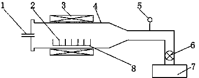
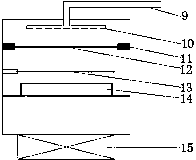
[0036] (1) Carry out anodic oxidation treatment on the cleaned p-type single crystal silicon wafer, the specific process is as follows: first pass a small current of 3mA for 30s to form a small hole layer on the surface of the silicon wafer; then pass a large current of 100mA for 50s, A macroporous layer is formed under the small pore layer. The solution used for anodic oxidation is 40% hydrofluoric acid and 99.9% absolute ethanol, and the volume ratio is 1:1.

[0037] (2) Anneal the silicon wafer after the above treatment in a hydrogen atmosphere to close the small pore layer and restore the single crystal structure. At the same time, the pore size of the large pore layer will increase to facilitate the layer transfer process. The specific process is as follows: pressure controlled at 3×10 3 Pa, the ...

Embodiment 2

[0051] Embodiment two: Put the remaining silicon wafer after stripping in Example 1 into a container containing 25% sodium hydroxide solution, heat the entire container to 80°C for 10 minutes, and then transfer the silicon wafer to 1% hydrofluoric acid Rinse in medium for 60s, and finally rinse with deionized water and blow dry with nitrogen. Then repeat the process of embodiment one.

[0052] Implementation results: tested at AM1.5, temperature 25°C, its Voc is 531mV, Jsc is 32.65mA / cm 2 , FF is 0.6755, η=11.7%.

Embodiment 3

[0053] Embodiment three: Put the remaining silicon wafer after stripping in Example 2 into a container with 25% sodium hydroxide solution, heat the entire container to 80°C for 10 minutes, and then transfer the silicon wafer to 1% hydrofluoric acid Rinse in medium for 60s, and finally rinse with deionized water and blow dry with nitrogen. Then repeat the process of embodiment one.

[0054] Implementation results: Tested at AM1.5, temperature 25°C, its Voc is 533mV, Jsc is 32.30mA / cm 2 , FF is 0.6761, η=11.6%.


PUM

PropertyMeasurementUnit
thicknessaaaaaaaaaa
thicknessaaaaaaaaaa
thicknessaaaaaaaaaa

Abstract

The invention relates to a heterojunction solar cell and a manufacturing method thereof and belongs to the technical field of solar cell apparatuses. The heterojunction solar cell is characterized in that: a first-type noncrystal silicon carbide layer is arranged between a transparent conductive film and a first-type noncrystal silicon and the thickness of the layer is 10 to 50nm; and a transparent conductive film is arranged between a quasi-monocrystal silicon layer and a metal film and the thickness of the layer is 100 to 300nm. The manufacturing method comprises the following steps of: manufacturing a double-layer porous silicon by using a p-type (or n-type) monocrystal silicon wafer, growing a p-type (or n-type) crystal silicon layer and an intrinsic crystal silicon layer successively after H2 annealing, performing H2 treatment on the surfaces of samples sequentially to manufacture the intrinsic crystal silicon layer, an n-type (or p-type) noncrystal silicon layer and an n-type (or p-type) noncrystal silicon carbide layer, and performing layer transfer after the manufacturing of an apparatus is finished. A silicon wafer can be reused on the premise of obtaining a high-quality silicon film; the conductivity and the transmissivity of a window layer are higher; and excellent electrode contact can be realized at a low temperature.

Description

technical field [0001] The invention belongs to the technical field of solar cell devices, and relates to a heterojunction solar cell prepared by using a porous silicon layer transfer technology and a preparation method thereof. Background technique [0002] A solar cell is a semiconductor device capable of converting light energy of sunlight into electrical energy. Because it does not need water, oil, gas or fuel, it can generate electricity as long as there is light. It can be called a clean, pollution-free renewable energy source and is favored by people. Solar cells are mainly made on the basis of semiconductor materials, and their working principle is that photoelectric conversion reactions occur after photoelectric materials absorb light energy to generate current. After more than half a century of development of solar cells, the conversion efficiency has increased by 5 times, and the production cost has also been reduced by 2 orders of magnitude compared with the pa...

Claims


Application Information

Patent Timeline
Patent Type & Authority Patents(China)
IPC IPC(8): H01L31/18H01L31/075
CPCY02E10/50Y02E10/548Y02P70/50
Inventor 沈鸿烈岳之浩张磊吴天如刘斌吕红杰
Owner NANJING UNIV OF AERONAUTICS & ASTRONAUTICS
Why Eureka
Try Eureka