Grid driving circuit, grid driving method, array substrate row driving circuit and display device

A gate drive circuit and gate technology, applied in the field of gate drive circuits, array substrate row drive circuits and display devices

Active Publication Date: 2014-04-09
BOE TECH GRP CO LTD
View PDF5 Cites 18 Cited by
  • Summary
  • Abstract
  • Description
  • Claims
  • Application Information

AI Technical Summary

Problems solved by technology

However, OLED's Vth compensation pixel design requires peripheral drive ci

Method used


Image

  • Grid driving circuit, grid driving method, array substrate row driving circuit and display device
  • Grid driving circuit, grid driving method, array substrate row driving circuit and display device
  • Grid driving circuit, grid driving method, array substrate row driving circuit and display device

Examples


Embodiment Construction

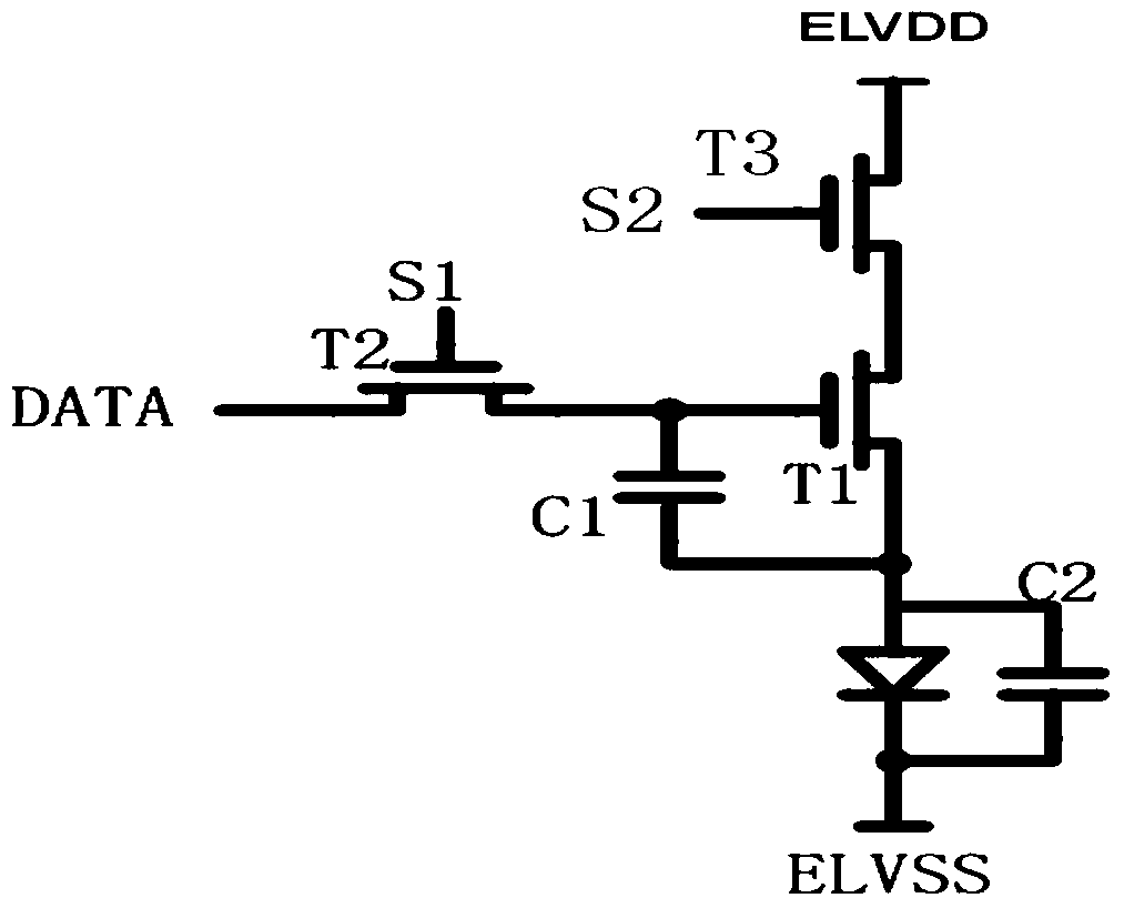
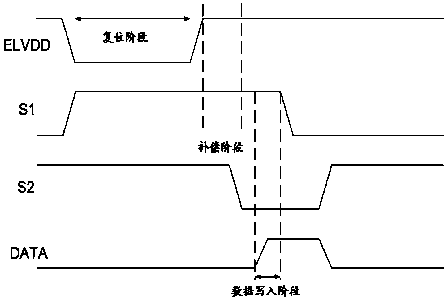
[0094] The gate driving circuit described in the embodiment of the present invention is connected to a row of pixel units, and the row of pixel units includes a row of pixel driving modules and light-emitting elements connected to each other; the row of pixel driving modules includes a driving transistor, a driving module and a compensation module; The compensation module is connected to the scanning signal of the first row; the driving module is connected to the scanning signal of the second row and the driving level;

[0095] The gate drive circuit further includes a row pixel control unit, which is configured to provide the compensation module with the first row scan signal, and provide the drive module with the second row scan signal and the drive level, The compensation module is controlled to compensate the threshold voltage of the driving transistor and the driving module is controlled to drive the light emitting element.

[0096] The gate drive circuit described in the...


PUM


Abstract

The invention provides a grid driving circuit, a grid driving method, an array substrate row driving circuit and a display device. The grid driving circuit is connected with a row pixel unit, the row pixel unit comprises a row pixel driving module and a light emitting component which are mutually connected, wherein the row pixel driving module comprises a driving transistor, a driving module and a compensation module, the compensation module is connected with the first row scanning signal, the driving module is connected with the second row scanning signal and a driving level, the grid driving circuit further comprises a row pixel control unit used for providing the first row scanning signal for the compensation module and used for providing the second row scanning signal and the driving level for the driving module, so the compensation module is controlled to compensate threshold voltage of the driving transistor, and the driving module is controlled to drive the light emitting component. The grid driving circuit can compensate the pixel threshold voltage and a driving pixel and improves an integration level.

Description

technical field [0001] The present invention relates to the field of display technology, in particular to a gate drive circuit, a method, an array substrate row drive circuit and a display device. Background technique [0002] There is no GOA (Gate on array, array substrate row drive) that can provide Vth (threshold voltage) compensation for OLED (Organic Light-Emitting Diode, Organic Light-Emitting Diode) display panel pixels. Array substrate) circuits, but only provide a pixel design with Vth compensation function or a single-pulse GOA circuit. [0003] Since the OLED pixel design mostly adopts the current control type, the Vth inhomogeneity in the entire OLED display panel and the Vth Shift (drift) generated after long-term operation will reduce the display uniformity of the OLED display panel. In order to improve the process integration of OLED display panels while reducing costs, the use of integrated gate drive technology is a future development trend. However, the V...

Claims


Application Information

Patent Timeline
IPC IPC(8): G09G3/32
CPCG09G3/3233G09G3/3266G09G3/3291G09G2300/0819G09G2300/0861G09G2300/0866G09G2310/0286G09G2320/043G11C19/28G09G3/3258G09G2300/043G09G2320/0295
Inventor 曹昆吴仲远段立业
Owner BOE TECH GRP CO LTD
Why Eureka
Try Eureka