Formation method of metal grid electrode

A metal gate and metal gate technology, which is applied in the direction of electrical components, semiconductor/solid-state device manufacturing, semiconductor devices, etc., can solve the problem that the metal gate is difficult to meet the process requirements, and achieve the goal of improving process integration and saving process steps Effect

Active Publication Date: 2013-05-15
SEMICON MFG INT (SHANGHAI) CORP
View PDF5 Cites 1 Cited by
  • Summary
  • Abstract
  • Description
  • Claims
  • Application Information

AI Technical Summary

Problems solved by technology

However, due to the different work functions of the NMOS transistor and the PMOS transistor, the materials and processes of the metal gate of the NMOS transistor and the metal gate of the PMOS transistor are different, and need to be formed separately, which makes the metal gate of the NMOS transistor and the PMOS transistor Difficult to meet process requirements

Method used


Image

  • Formation method of metal grid electrode
  • Formation method of metal grid electrode
  • Formation method of metal grid electrode

Examples


Embodiment Construction

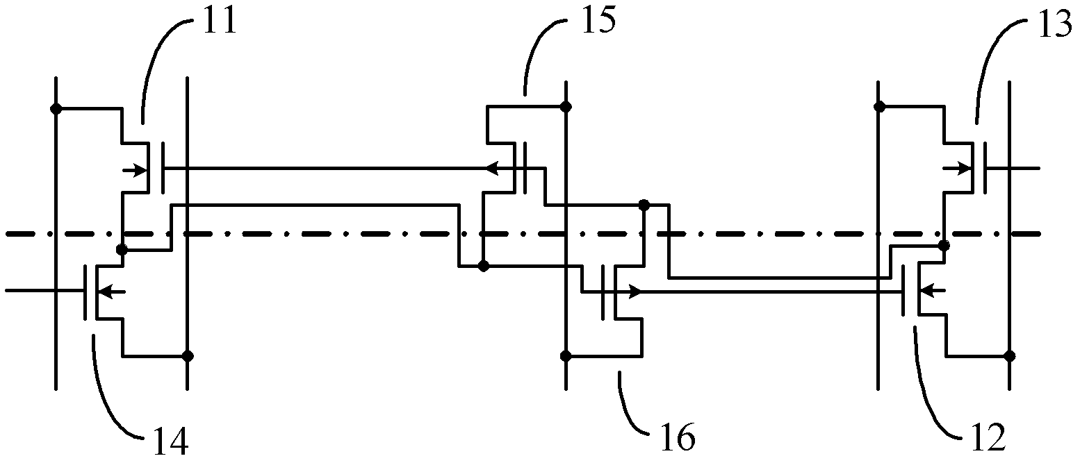
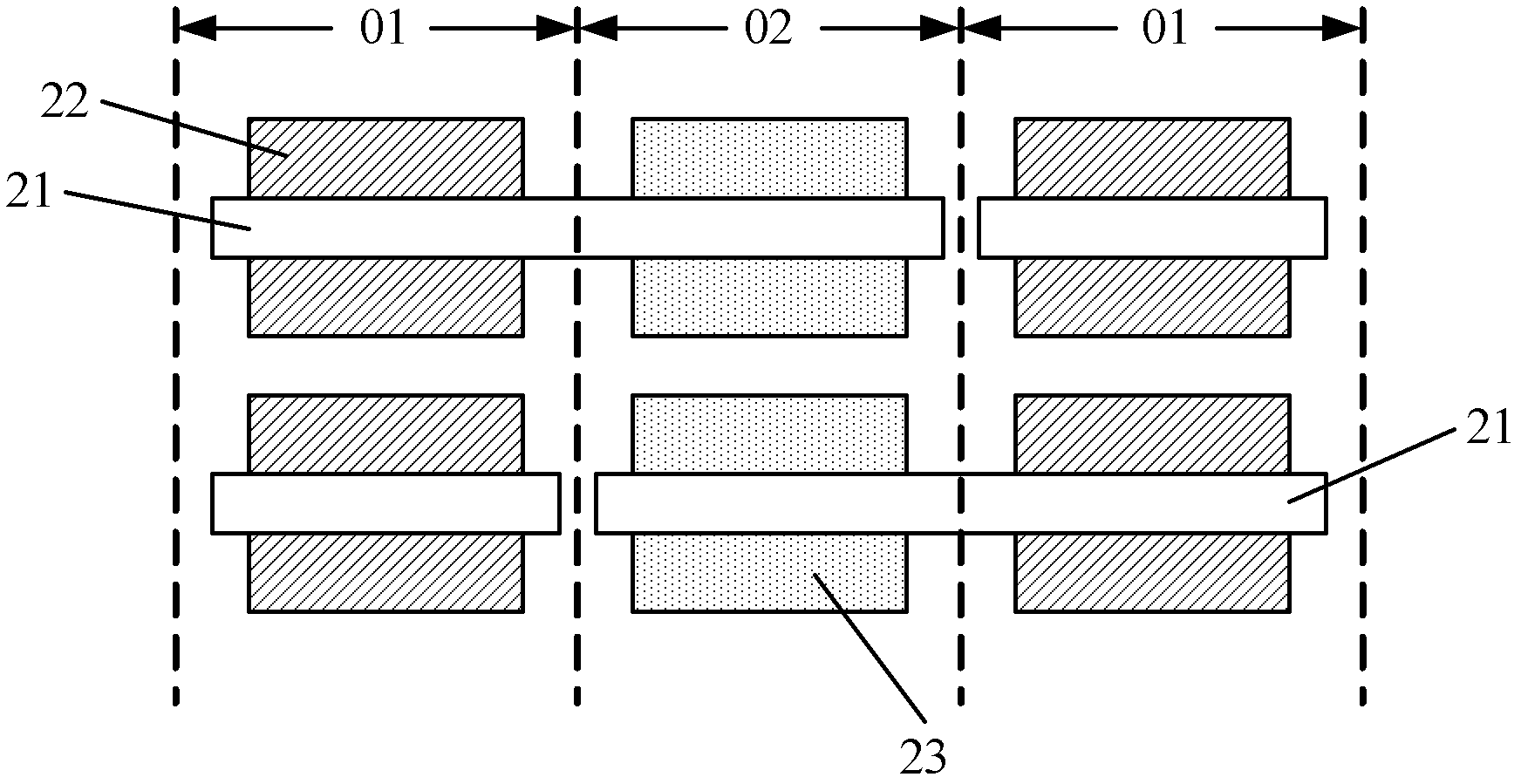
[0041] In existing SRAM memory cells, the gate of an NMOS transistor is usually electrically connected to the gate of a PMOS. In order to improve device integration and avoid the formation of conductive plugs on the surface of the gate structure, in layout design, an NMOS transistor and a PMOS transistor usually share the same gate structure. For details, please refer to figure 2, which is a structural schematic diagram of the common gate of the NMOS transistor and the PMOS transistor in the SRAM memory unit of the prior art, including: an NMOS transistor region 01 and a PMOS transistor region 02 are provided on the semiconductor substrate; the common gate 21 spans the NMOS Transistor region 01 and the boundary of PMOS transistor region 02, a part of the common gate 21 is located in the NMOS transistor region 01, and another part of the common gate 21 is located in the PMOS transistor region 02; in the NMOS transistor region 01, all N-type source / drain regions 22 are formed o...


PUM


Abstract

Disclosed is a formation method of a metal grid electrode. The formation method of the metal grid electrode comprises that a semi-conductor substrate is provided. The semi-conductor substrate comprises a first transistor area and a second transistor area. A polycrystalline silicon thin film is formed on the semi-conductor substrate. Ion implantation is carried out on a polycrystalline silicon thin film in the first transistor area. Part of the polycrystalline silicon thin film is eliminated so that a replacing grid electrode structure is formed. The replacing grid electrode structure is arranged in the first transistor area and the second transistor area at the same time. Tetramethylammonium hydroxide liquor is used for eliminating the replacing grid electrode structure of the second transistor area. The ion implantation is not carried out in the second transistor area. A second groove is formed. A second metal grid electrode is formed in the second groove. The replacing grid electrode structure of the first transistor area is eliminated. The ion implantation is carried out in the first transistor area. A first groove is formed. A first metal grid electrode is formed in the first groove. Due to the fact that the replacing grid electrode structure is etched selectively by the tetramethylammonium hydroxide liquor, a perpendicular groove side wall can be achieved by taking advantage of the ion implantation, thus technological requirements can be met by the follow-up formed metal grid electrode.

Description

technical field [0001] The invention relates to the field of semiconductor manufacturing, in particular to a method for forming a metal gate. Background technique [0002] With the continuous development of integrated circuit manufacturing technology, the feature size of MOS transistors is getting smaller and smaller. In order to reduce the parasitic capacitance of the gate of MOS transistors and improve the device speed, the gate stack of high K gate dielectric layer and metal gate structure is introduced into MOS transistors. In order to avoid the influence of the metal material of the metal gate on other structures of the transistor, the gate stack structure of the metal gate and the high-K gate dielectric layer is usually fabricated by a “gate last” process. [0003] US Patent Publication No. US2002 / 0064964A1 discloses a method of forming a metal gate using a "gate-last" process, comprising: providing a semiconductor substrate on which a replacement gate structure is fo...

Claims


Application Information

Patent Timeline
Patent Type & Authority Applications(China)
IPC IPC(8): H01L21/28H01L21/8238H01L21/336H01L21/3213
Inventor 何其旸
Owner SEMICON MFG INT (SHANGHAI) CORP
Why Eureka
Try Eureka