Method for avoiding metal line short circuit in OLED display device

A technology for metal circuits and display devices, which is applied in the field of avoiding short circuits of metal circuits in OLED display devices, can solve problems such as time-consuming and labor-intensive, and can not fully achieve the expected effect, and achieve the effect of avoiding short circuits.

Active Publication Date: 2014-04-09
TCL CHINA STAR OPTOELECTRONICS TECH CO LTD
View PDF4 Cites 10 Cited by
  • Summary
  • Abstract
  • Description
  • Claims
  • Application Information

AI Technical Summary

Problems solved by technology

However, in the actual production process, due to the limitation of process conditions, this method cannot fully achieve the expected effect, and it is labor-intensive and time-consuming.

Method used


Image

  • Method for avoiding metal line short circuit in OLED display device
  • Method for avoiding metal line short circuit in OLED display device
  • Method for avoiding metal line short circuit in OLED display device

Examples


Embodiment Construction

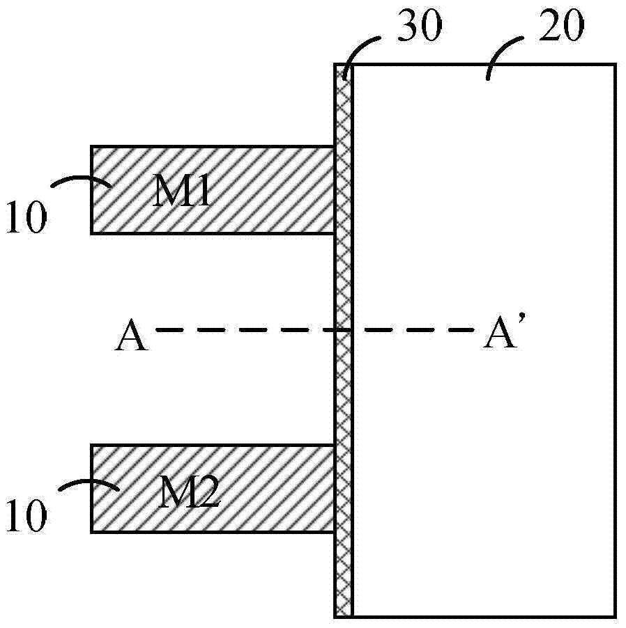
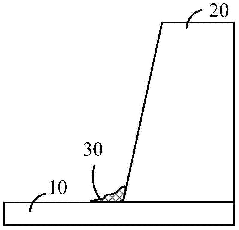
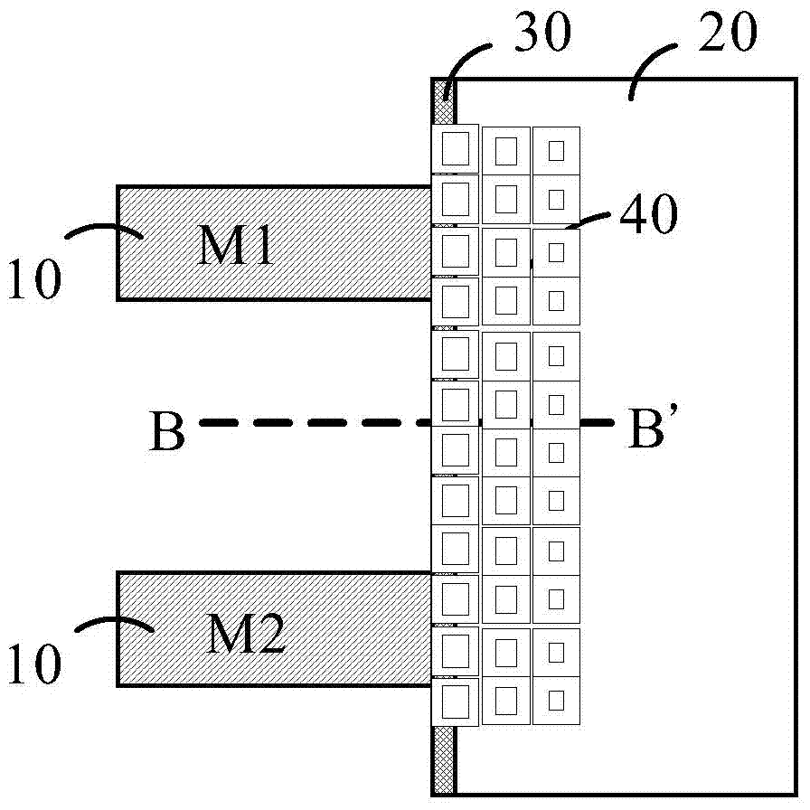
[0032] Such as image 3 As shown, it is a flow chart of the method proposed by the present invention for avoiding the short circuit of the metal circuit in the OLED display device. In order to further illustrate the purpose of the present invention, technical scheme and the technical effect that reaches, below in conjunction with non-limiting embodiment, and Figure 4A and 4B , Figure 5A and 5B Make a detailed introduction. The directional terms mentioned therein, such as up, down, front, back, left, right, inside, outside, side, etc., are only directions referring to the attached drawings. Therefore, the used directional terms are only used to illustrate and understand the present invention, but not to limit the present invention.

[0033] Step S100, providing a substrate.

[0034] Step S102, forming a gate layer and a semiconductor layer on the substrate.

[0035] Step S103, forming an inorganic layer on the substrate.

[0036] Wherein, it should be noted that the r...


PUM


Abstract

The invention relates to a method for avoiding metal line short circuit in an OLED display device. The method comprises the steps that an inorganic layer is formed on a substrate; a patterned metal layer is formed on the inorganic layer; the patterned metal layer comprises more than two metal lines; a patterned organic layer is formed on the patterned metal layer; an island area with low height is between every two adjacent metal lines on the edge of the patterned organic layer; and an ITO layer is formed on the patterned organic layer. According to the invention, the island areas with low height are arranged on the edge of the organic layer, thus ITO parts deposited on the edge of the organic layer are deposited on the island areas; the ITO on the island areas can be completely etched and removed in a later lithography process; and the residual ITO on the edge of the organic layer is no longer continuous between two adjacent metal lines, thus the situation of short circuit of two adjacent metal lines, which is caused by the residual ITO, is avoided.

Description

technical field [0001] The invention relates to a manufacturing process of a semiconductor display panel, in particular to a method for avoiding short circuit of a metal circuit in an OLED display device. Background technique [0002] Indium tin oxide (ITO) thin film is widely used in high-tech products such as semiconductor display panels due to its excellent electrical conductivity and light transmittance, good adhesion and stability to substrates, and good etching properties. Fabricate transparent electrodes. For example, it is fabricated as an anode in an OLED display device (Organic Light-Emitting Diode, Organic Light-Emitting Diode). The manufacturing process of the OLED display device is roughly divided into two parts: manufacturing several thin film transistors on a substrate as switching elements, and manufacturing organic light emitting diodes as light emitting elements. Such as Figure 1A As shown, a gate layer (not shown in the figure) and a semiconductor layer...

Claims


Application Information

Patent Timeline
Patent Type & Authority Applications(China)
IPC IPC(8): H01L21/82H05B33/10
CPCH10K71/621H10K50/816H10K2102/341H01L27/1244H01L27/1288H10K59/124H10K59/131H10K71/00H10K59/1201
Inventor 柯凯元
Owner TCL CHINA STAR OPTOELECTRONICS TECH CO LTD
Why Eureka
Try Eureka