OLED display panel and manufacturing method thereof

A technology for display panels and manufacturing methods, which is applied in semiconductor/solid-state device manufacturing, organic semiconductor devices, semiconductor devices, etc., and can solve problems such as total reflection on the light-emitting side

Active Publication Date: 2014-04-09
BOE TECH GRP CO LTD
View PDF11 Cites 28 Cited by
  • Summary
  • Abstract
  • Description
  • Claims
  • Application Information

AI Technical Summary

Problems solved by technology

[0006] The technical problem solved by the present invention is: how to provide an OLED display panel and its manufacturing method, so as to solve the problem of total reflection on the light-emitting side in the prior art

Method used


Image

  • OLED display panel and manufacturing method thereof
  • OLED display panel and manufacturing method thereof
  • OLED display panel and manufacturing method thereof

Examples


Embodiment Construction

[0034] The specific implementation manners of the present invention will be further described in detail below in conjunction with the accompanying drawings and embodiments. The following examples are used to illustrate the present invention, but are not intended to limit the scope of the present invention.

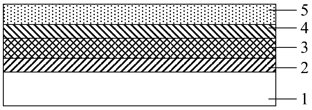
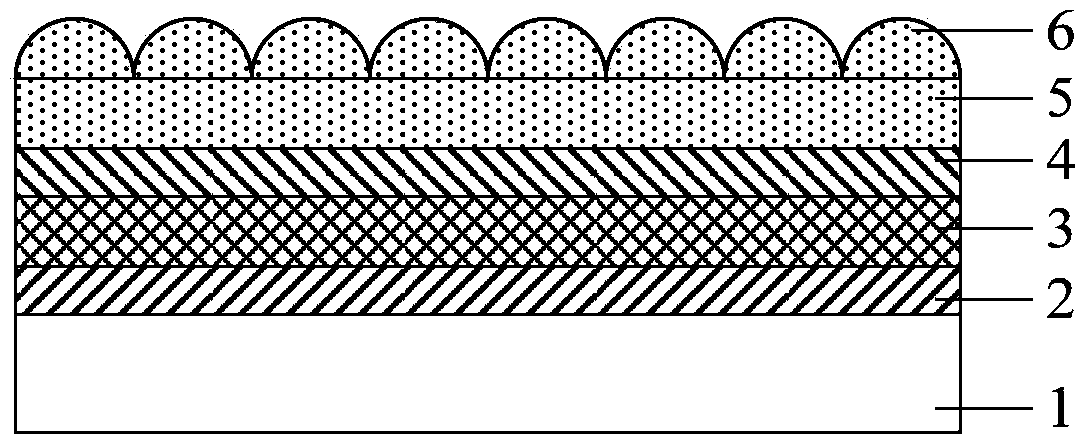
[0035] A method for manufacturing an OLED display panel provided by an embodiment of the present invention, such as figure 2 As shown in the OLED display panel, the method includes:

[0036] Step S1 , a step of sequentially forming an anode 2 , an organic light-emitting layer 3 , a cathode 4 and a first optical coupling layer 5 on the base substrate 1 . Each pixel of the OLED display panel includes a corresponding anode 2 , an organic light emitting layer 3 , a cathode 4 and a first light coupling layer 5 . In this step, the anode 2, the organic light-emitting layer 3, the cathode 4, and the first optical coupling layer 5 are made by using an existing common mask, throu...


PUM


Abstract

The invention provides a manufacturing method of an OLED display panel. The method comprises the step of sequentially forming an anode, an organic light-emitting layer, a cathode and a first optical coupling layer on a substrate, and further comprises the step of forming a second optical coupling layer formed by arranging a plurality of protrusion structures with the arc-shaped surfaces on one side, away from the cathode, of the first optical coupling layer. The invention further provides the OLED display panel. According to the method, light rays are transmitted out through the protrusion structures with the arc-shaped surfaces of the second optical coupling layer, wherein total reflection of the light rays will happen to the surface of the first optical coupling layer originally, therefore the total reflection of the light is reduced, the take-out rate of the light is increased, and the external quantum efficiency of the OLED display panel is improved.

Description

technical field [0001] The invention relates to the field of preparation of organic photoelectric devices, in particular to an OLED display panel and a manufacturing method thereof. Background technique [0002] OLED (Organic Light-Emitting Diode, Organic Light-Emitting Diode) has many advantages such as self-illumination, all-solid-state, wide viewing angle, fast response, etc., and has a huge application prospect in flat panel display. OLED is considered to be the successor to LCD (Liquid Crystal Display, Liquid crystal display), PDP (Plasma Display Panel, plasma display panel), a new generation of flat panel display products and technologies. At present, OLEDs are widely used in display and lighting fields. In order for semiconductor light-emitting elements to ensure high functional reliability and low energy consumption, it is necessary to increase the external quantum efficiency (External quantum efficiency) of the element itself. In general, the external quantum effi...

Claims


Application Information

Patent Timeline
Patent Type & Authority Applications(China)
IPC IPC(8): H01L51/56H01L51/52H01L27/32
CPCH10K59/00H10K50/858H10K71/00H10K2102/00
Inventor 张粲
Owner BOE TECH GRP CO LTD
Why Eureka
Try Eureka