Package Test Method

A technology of packaging testing and packaging components, which is applied in semiconductor/solid-state device testing/measurement, electrical components, semiconductor/solid-state device manufacturing, etc., can solve the technical difficulties of chip electrical isolation, production cost and time waste, and achieve Reduce costs, improve usage flexibility, and simplify processes

Active Publication Date: 2018-04-03
WINBOND ELECTRONICS CORP
View PDF5 Cites 0 Cited by
  • Summary
  • Abstract
  • Description
  • Claims
  • Application Information

AI Technical Summary

Problems solved by technology

Existing test systems are mostly suitable for package structures with leads, such as Small Outline Package and Quad Flat Package (QFP), etc., but for leadless package structures, such as: Small Outline No-Lead (SON) and Quad Flat No-lead (QFN), etc., have difficulties in the process of electrically isolating chips
In addition, in traditional package testing, the test system needs to prepare corresponding pick-up equipment and carrying fixtures for different package structure sizes, which requires additional processes or the purchase of expensive equipment and fixtures, which has a huge impact on production costs and time. kind of waste

Method used


Image

  • Package Test Method
  • Package Test Method
  • Package Test Method

Examples


Embodiment Construction

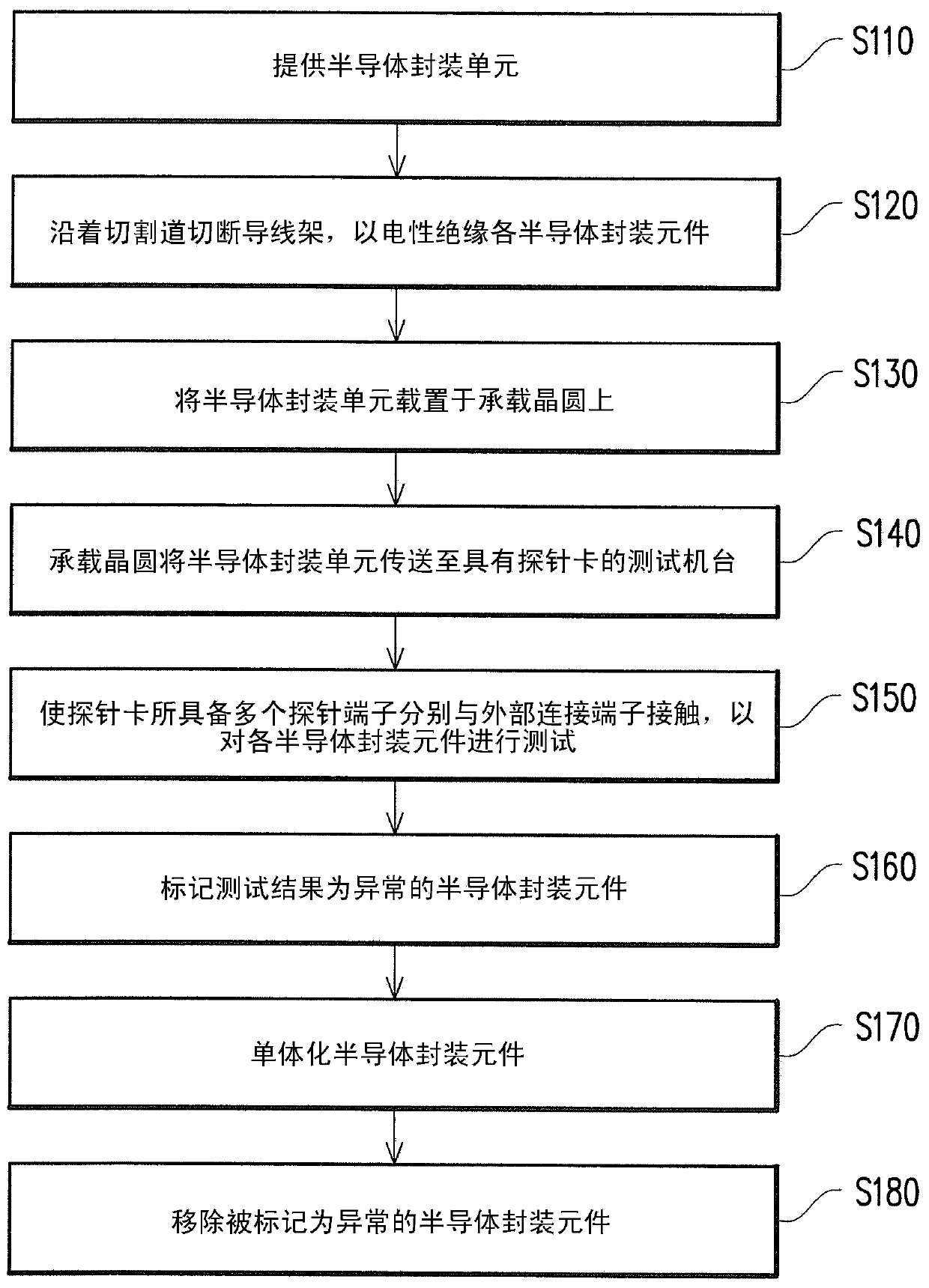
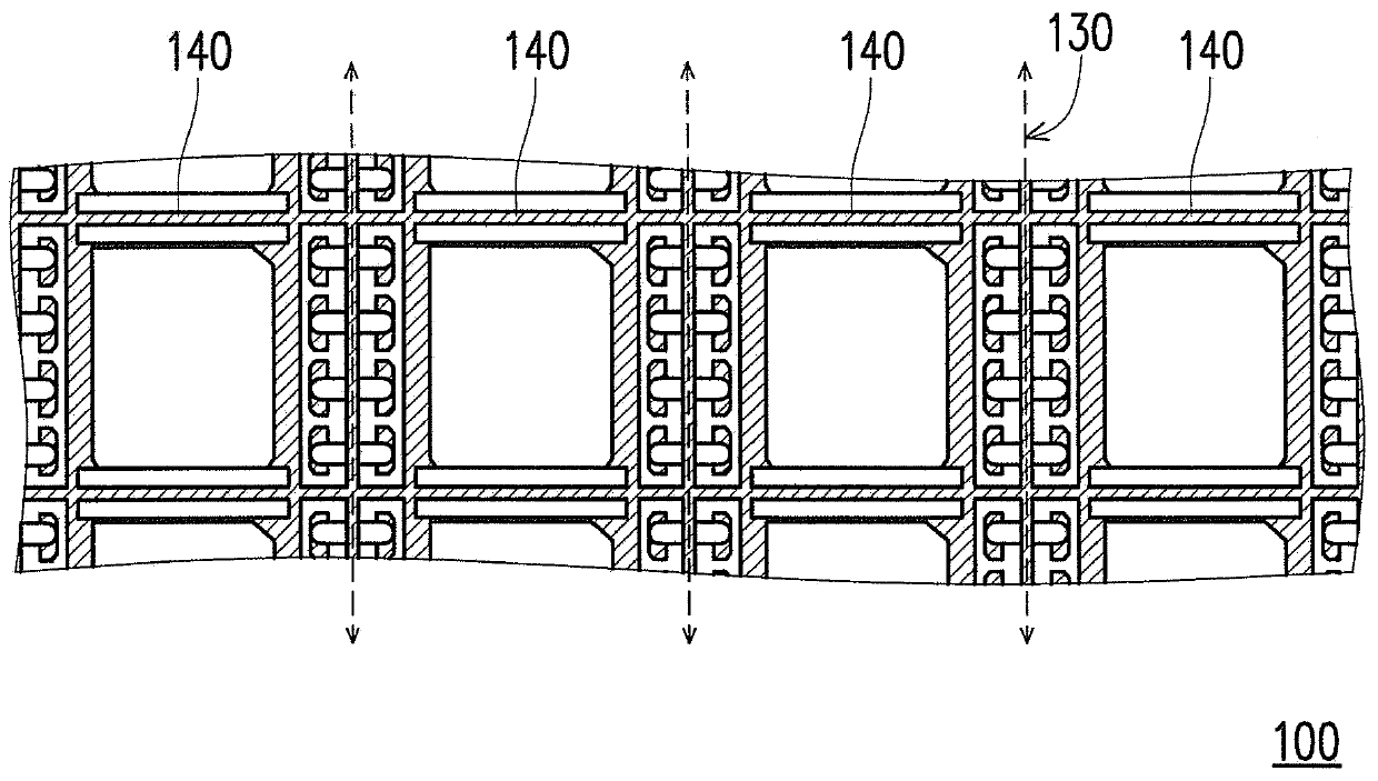
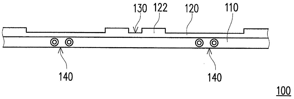
[0034] figure 1 It is a schematic flowchart of a packaging and testing method according to an embodiment of the present invention. figure 2 It is a partial schematic diagram of a semiconductor package unit according to an embodiment of the present invention. image 3 is a schematic cross-sectional view of a semiconductor package unit according to an embodiment of the present invention. Please also refer to figure 1 , figure 2 and image 3 , the packaging and testing method of this embodiment is suitable for performing a yield test on a semiconductor packaging unit 100, and the packaging and testing method includes the following steps: first, step S110 is performed, and the following steps are provided: figure 2 and image 3 A semiconductor package unit 100 is shown, which includes an encapsulant 110 , a lead frame 120 and a plurality of dicing lines 130 . The dicing line 130 defines a plurality of semiconductor package elements 140 on the semiconductor package unit 10...


PUM


Abstract

The invention discloses a packaging and testing method, which includes the following steps. A semiconductor package unit is provided, which includes a package compound, a lead frame and a plurality of dicing lines. The dicing line defines a plurality of semiconductor package elements on the semiconductor package unit. Each semiconductor package element has a plurality of external connection terminals. The lead frame is cut along the dicing line to electrically insulate the semiconductor package components. The semiconductor packaging unit is placed on the carrier wafer. The probe card is brought close to the semiconductor package unit mounted on the carrier wafer, and the plurality of probe terminals of the probe card are respectively contacted with the external connection terminals, so as to test each semiconductor package element. Mark test results as abnormal semiconductor package components. Singulating the semiconductor package components and removing the semiconductor package components marked as abnormal.

Description

technical field [0001] The present invention relates to a testing method, and in particular to a packaging and testing method of a semiconductor element. Background technique [0002] In order to obtain information on the pros and cons of the process at any time during the manufacturing process of semiconductor package components, multiple test keys are specially designed on the semiconductor package components, and these test keys are then connected through test terminals and subjected to various tests , to monitor the pros and cons of each stage of the process. [0003] After the semiconductor element is covered with encapsulant and before electroplating, each chip on the lead frame is electrically short-circuited. Therefore, if you want to test with a semiconductor package unit that has not been singulated (Singulation), you must first complete its Electrical isolation between chips. [0004] Compared with the testing method of singulated wafers, the testing method of t...

Claims


Application Information

Patent Timeline
Patent Type & Authority Patents(China)
IPC IPC(8): H01L21/50H01L21/56H01L21/66
Inventor 傅廷明
Owner WINBOND ELECTRONICS CORP
Why Eureka
Try Eureka