Method for selectively removing conductive layer on baseplate material

A conductive layer, selective technology, applied in electrical components, printed circuits, printed circuit manufacturing, etc., can solve the problems of short laser projection path, difficult to peel off, and high temperature at the end of laser heating, and achieve a simple and fast circuit structure. , Avoid oxidation and burns, reduce the effect of oxidation and burns

Active Publication Date: 2014-04-23
德中(天津)技术发展股份有限公司
View PDF5 Cites 10 Cited by
  • Summary
  • Abstract
  • Description
  • Claims
  • Application Information

AI Technical Summary

Problems solved by technology

[0026] It can be seen that the method described in DE 10 2010 019 406 A1 adopts a strip-shaped conductive layer separation scheme. Since the heat dissipation conditions of each part in the middle of the small block are basically the same, and the heat dissipation conditions at the terminal end are poor, it is not conducive to the transfer of heat at the high temperature end. The temperature difference of each part of the conductive layer is enlarged
This difference causes the temperature of the termination end of laser heating to be too high, so that it affects the adjacent wires to be retained, and the phenomenon of those long-length strip-shaped conductive layer pieces is more prominent.
These small pieces, because of their long length, are heavy and are not easily excluded by the airflow. In addition, the temperature of the terminal end is too high, which is more likely to affect the adjacent wires to be retained, or melt with the conductive layer that has not been removed after falling off. Together, stay on the substrate material, affect further laser projection, and also affect the quality of the conductive structure
[0027] A further problem is that DE 10 2010 019 406 A1 subdivides the conductive layer to be removed into small strips with the same width everywhere and equal width to each other. When heating the long strips, the terminal temperature exceeds The temperature required to peel off small pieces cannot make full use of the energy delivered by the laser to the processed material, and the processing efficiency is still not high enough
On the other hand, when the strip-shaped small pieces do not reach a certain length, although the laser transmits the same amount of energy per unit time to the unit length during heating, the time and path of the laser action will also be too short to make the small pieces The temperature of the end point rises to the point where the adhesion decreases and the stress increases, causing it to fall off the substrate
[0028] The problem of this subdivision method is not only that, according to the subdivision of the so-called main axis of the wiring at an acute angle of 22.5°, the same width everywhere, and the small pieces of the separated conductive layer of equal width will result in the middle of the conductive layer pattern to be retained, or Between the conductive layer and the edge, isolated small pieces are often left, the length or width of which is smaller than most separated strips of conductive layer pieces
Such a small piece is difficult to be peeled off during subsequent heating
Obviously, the size of the isolated small pieces left by this separation method is smaller than that of the usual strip-shaped small pieces. Although the laser transmits the same amount of energy per unit time to the unit length during heating, the laser projection path is shorter, making the end point Insufficient temperature rise at the tip to cause nubs of the conductive layer to detach from the substrate material
[0029] Another problem is that, according to the method described in DE 10 2010 019 406 A1, during processing, the compressed air plays an upward component force to peel off the strip-shaped pieces of the conductive layer, which plays an important role in removing the specified conductive layer, but in In practice, the wires will be burned and the surface will be discolored.

Method used


Image

  • Method for selectively removing conductive layer on baseplate material

Examples


Embodiment

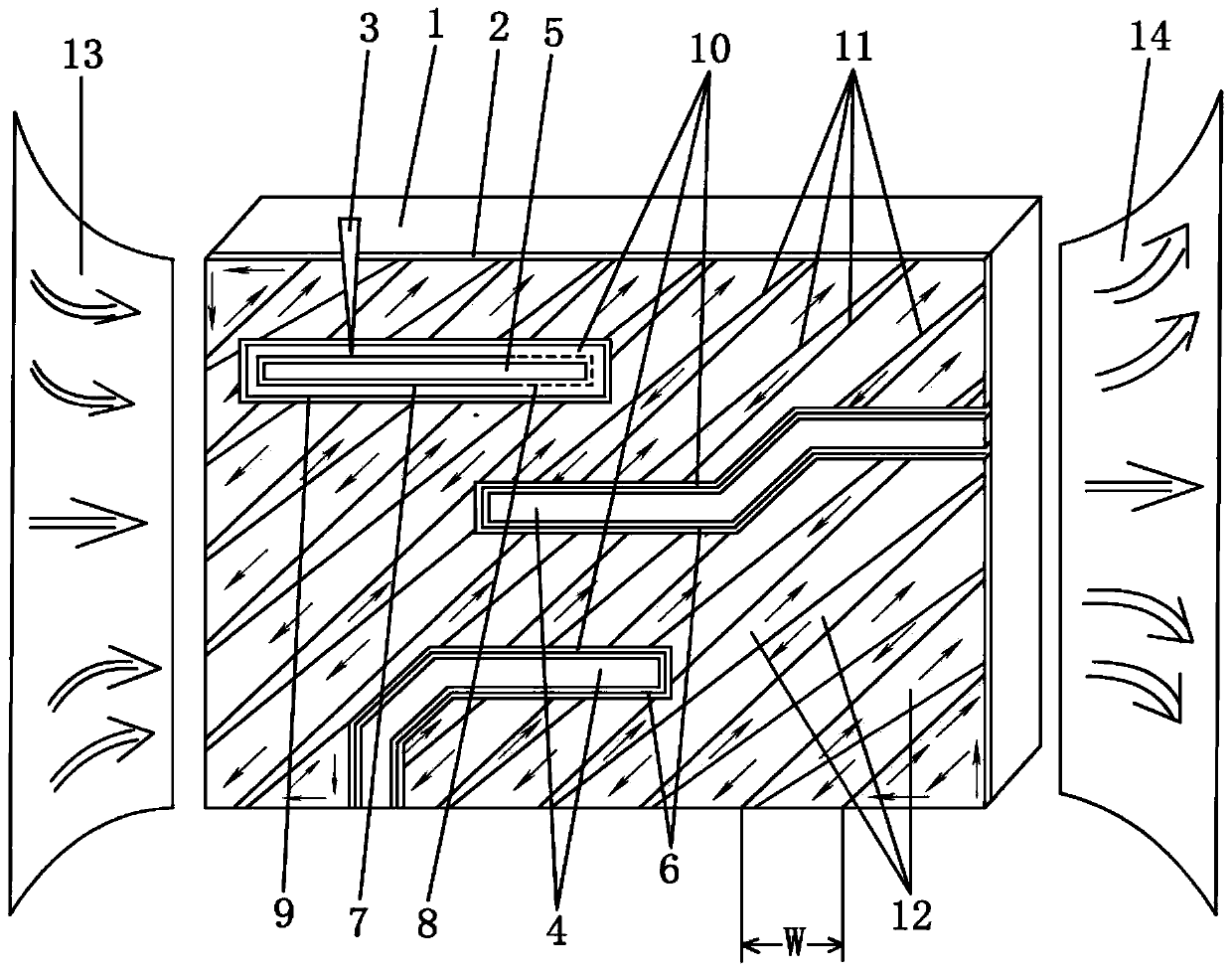
[0062] In this example, the substrate material is FR4 copper-clad laminate, using CircuitCAM V7.0 or above or DCT-DreamCreaTor software to process the data to be processed, and using DCT-DL500 laser equipment for processing.

[0063] A method for selectively removing the conductive layer on the substrate material according to design requirements to form a predetermined conductive pattern. In the method, the insulation channel path, the separation path and the heating path are as follows: figure 1 As shown, wherein, 1 is an insulating substrate material, and 2 is a metal conductive layer covering the substrate material. The operation steps are:

[0064] Step (1): Under the condition that the dust collection device 14 is turned on and the inert gas delivery device 13 is turned on, use a laser to process the insulating channel on the outer edge of the conductive layer to be retained;

[0065] First process the ultra-narrow isolated wire 5, and use the laser beam 3 to complete par...


PUM


Abstract

The invention relates to a method for selectively removing a conductive layer on a baseplate material. The method comprises the following steps: processing to manufacture an insulated enveloping channel on the periphery of a to-be-reserved conductive layer, wherein an isolated wire with over-narrow width is processed twice or more than twice; subdividing a to-be-removed conductive layer into a plurality of insulated small blocks, wherein the adjacent insulated small blocks are of complementary shapes such as inverted quadrangle, trapezoid or triangle; projecting electromagnetic waves onto the subdivided insulated small blocks so as to ensure that the subdivided insulated small blocks are separated from the baseplate material to be removed, wherein during heating, the projected laser moves from the narrower end of each small block of the conductive layer to the wider end of each small block. According to the method, the projecting parameter, projecting path and projecting environment of the laser are regulated and the conductive layer on the substrate material is removed, so that a preset conductive structure is formed, and the method can be used for replacing a corresponding technical process adopted in the process of manufacturing a conductive structure by virtue of an existing chemical method, an existing physical method and an existing laser method.

Description

technical field [0001] The invention belongs to the technical field of circuit board processing, in particular to a method for selectively removing a conductive layer on a substrate material. Background technique [0002] Selective removal of the conductive layer on the specified area of ​​the metal-clad substrate material is one of the key steps in the subtractive method of manufacturing circuit boards, usually by chemical etching. That is, first transfer the pattern on the surface of the copper clad laminate, cover the conductive layer of the conductive pattern part that needs to be retained, usually copper foil, with a protective material-resist, and remove the non-conductive pattern part. The copper is exposed. During etching, the etchant and the exposed metal copper contact each other and react, and the copper is dissolved into the etchant solution to achieve the purpose of removal. [0003] The etching method has a long and complicated process, and requires a lot of ...

Claims


Application Information

Patent Timeline
Patent Type & Authority Applications(China)
IPC IPC(8): H05K3/02
Inventor 胡宏宇洪少彬
Owner 德中(天津)技术发展股份有限公司
Why Eureka
Try Eureka