Thermal resistance measuring method for semiconductor device

A test method and semiconductor technology, applied in the direction of single semiconductor device testing, material thermal development, etc., to achieve a wide range of applications

Active Publication Date: 2014-05-14
CHINA ACADEMY OF SPACE TECHNOLOGY
View PDF7 Cites 31 Cited by
  • Summary
  • Abstract
  • Description
  • Claims
  • Application Information

AI Technical Summary

Problems solved by technology

[0007] In order to solve the problem that integrated circuit products cannot directly use the transient thermal response test technology based on the electrical method to test thermal parameters, the application provides a thermal resistance test method for semiconductor devices, which is characterized in that it includes the following steps: 1) According to the semiconductor The structure of the device, determine the main heat conduction channel, and set a constant temperature plane with good contact on the shell surface of the main heat conductio...

Method used


Image

  • Thermal resistance measuring method for semiconductor device
  • Thermal resistance measuring method for semiconductor device
  • Thermal resistance measuring method for semiconductor device

Examples


Embodiment Construction

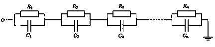
[0023] Thermal resistance refers to the resistance encountered when heat flows through a heat conductor. For semiconductor devices, a certain amount of power (especially power devices) must be applied during their operation, and most of this power is converted into heat, resulting in temperature rise of the device. The heat on the chip is transferred to the casing through the packaging material, and further transferred to the surrounding air environment (for devices with relatively high power, there will also be a heat sink). The unit of thermal resistance is ℃ / W or K / W, which means the temperature difference between the chip junction temperature of the device and the thermal reference point (ambient temperature or device case temperature) when the power is increased by 1W.

[0024] According to JEDEC standard No.51-1, the definition of thermal resistance of semiconductor devices is shown in Equation 1:

[0025] R θJX = (1)

[0026] R θJX is the thermal resistance of ...


PUM


Abstract

The invention relates to a thermal resistance measuring method for a semiconductor device. The thermal resistance measuring method includes the following steps that (1) according to the structure of the semiconductor device, a main heat conduction channel is determined, and a constant temperature plane good in contact is arranged on the surface of a shell of the main heat conduction channel; (2) certain power is loaded to the semiconductor device, after the semiconductor device reaches heat balance, it is switched to the situation that measuring power is loaded to the semiconductor device, temperature-sensitive parameters of the semiconductor device are measured in real time to obtain the junction temperature for measuring the semiconductor device, and accordingly a transient thermal response curve of the semiconductor device is obtained; (3) according to the transient thermal response curve, the thermal resistance from a junction of the semiconductor device to the shell is determined. According to the thermal resistance measuring method for the semiconductor device, heating power is loaded through a P zone and an N zone of a substrate of the semiconductor device, the junction temperature is measured by the utilization of a PN junction assembly existing in the semiconductor device, and therefore the transient thermal resistance of integrated circuit products without temperature-sensitive diodes and the transient thermal resistance of non-power integrated circuit products can be measured accurately.

Description

technical field [0001] The invention relates to a thermal resistance test method of a semiconductor device, which is particularly suitable for the transient thermal resistance test of integrated circuit products. Background technique [0002] Temperature is an important factor affecting the characteristics of semiconductor devices. When the device is working, too high junction temperature will have many adverse effects on the device, such as reduced performance, reduced reliability, and shortened lifespan. With the development of devices to small size and high integration, the power density carried in a limited space is getting higher and higher. This puts forward more and more urgent requirements for the research on the working temperature of semiconductor devices. First of all, it is necessary to accurately grasp the thermal resistance value of each electronic component in the system in order to conduct accurate thermal analysis and thermal management for the system. ...

Claims


Application Information

Patent Timeline
IPC IPC(8): G01R31/26G01N25/20
Inventor 张红旗唐章东王征宁永成张延伟焦景勇张洪硕曹玉生
Owner CHINA ACADEMY OF SPACE TECHNOLOGY
Why Eureka
Try Eureka