System and method for providing a digital self-adjusting power supply that provides a substantially constant minimum supply voltage with regard to variations of PVT, load, and frequency

a technology of digital self-adjusting and power supply voltage, applied in the direction of electric variable regulation, process and machine control, instruments, etc., can solve the problems of non-uniformity of process parameters within a single die, increase in power consumption per die, and differences in transistor and interconnect characteristics across the single di

Active Publication Date: 2009-10-13
NAT SEMICON CORP
View PDF6 Cites 50 Cited by
  • Summary
  • Abstract
  • Description
  • Claims
  • Application Information

AI Technical Summary

Problems solved by technology

As the number of transistors per integrated circuit chip has continued to increase, two critical circuit design issues have been presented.
The first design issue is the non-uniformity of process parameters within a single die.
The second design issue is the increment in power consumption per die.
In deep sub-micron circuit design, variations due to the non-uniformity of process parameters within a single die cause differences in transistor and interconnect characteristics across the single die.
These differences in turn negatively impact the performance of the circuit because they generate deviations in MOSFET (Metal Oxide Semiconductor Field Effect Transistor) drive current.
This results in propagation delay distributions of the critical path across a chip.
After fabrication, operating variations such as power supply voltage, chip temperature, and across-chip temperature also affect the magnitude of the propagation delay.
As a result, any transient introduced to the system, such as a start up transient or a load transient, causes a disturbance.
One drawback of switching converter 100 is that diode D introduces an undesirable resistance.
Another drawback of switching converter 100 is that the converter requires a band gap reference voltage source to respond to changes in PVT.
A band gap reference voltage source, however, is a complex circuit that provides only a roughly constant voltage over changes in PVT.
A further drawback of switching converter 100 is that switching converter 100 requires a proportional integrator differentiator (PID), which is also a complex circuit, in order to compensate for the second order effects of the LC network.
The implementation of a PID circuit adds a heavy hardware burden because a PID control law is typically expressed as a current and prior values of duty ratio, and error, and includes coefficients that require evaluation using multiplication.

Method used


Image

  • System and method for providing a digital self-adjusting power supply that provides a substantially constant minimum supply voltage with regard to variations of PVT, load, and frequency
  • System and method for providing a digital self-adjusting power supply that provides a substantially constant minimum supply voltage with regard to variations of PVT, load, and frequency
  • System and method for providing a digital self-adjusting power supply that provides a substantially constant minimum supply voltage with regard to variations of PVT, load, and frequency

Examples


Embodiment Construction

[0059]FIGS. 2 through 17, discussed below, and the various embodiments used to describe the principles of the present invention in this patent document are by way of illustration only and should not be construed in any way to limit the scope of the invention. Those skilled in the art will understand that the principles of the present invention may be implemented in any type of suitably arranged electronic device.

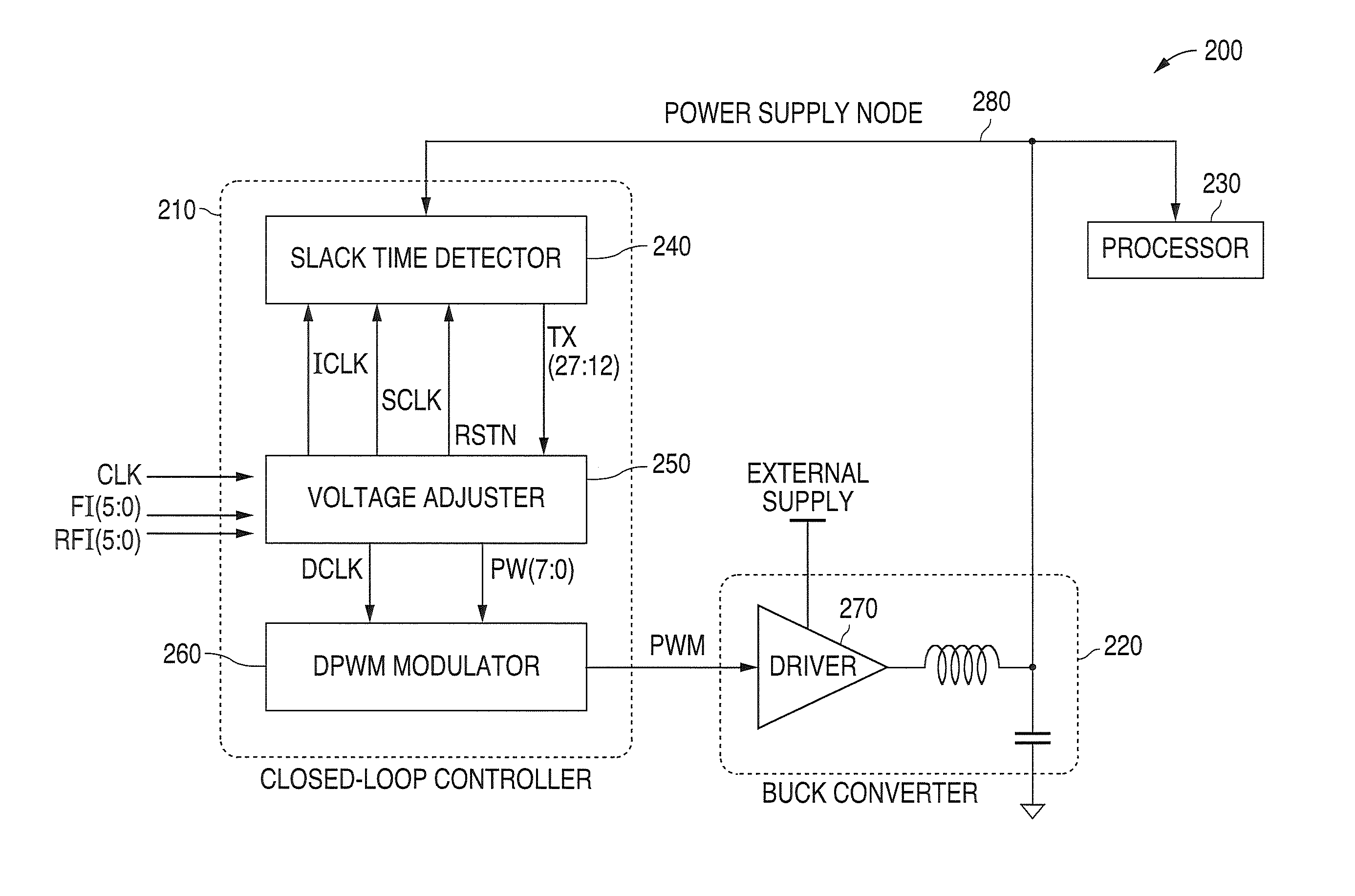
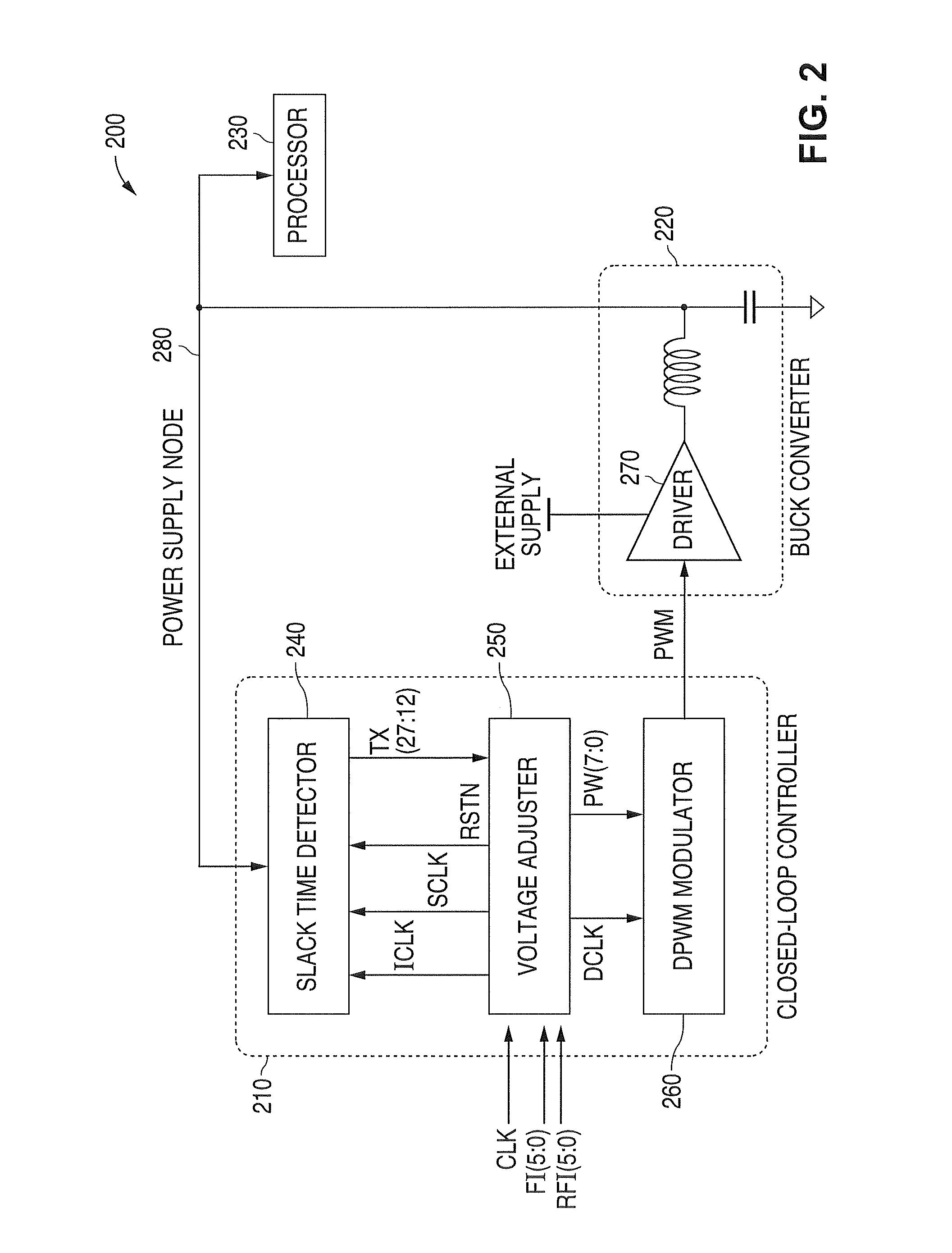
[0060]FIG. 2 is a block diagram illustrating a digital self adjusting minimum power supply system 200 in accordance with the principles of the present invention. The system 200 comprises a closed loop controller 210 that receives a fixed frequency clock signal CLK and frequency information FI(5:0), a DC-DC buck converter 220, and a processor 230 as a load current source. The closed loop controller 210 comprises a slack time detector 240, a voltage adjuster 250, and a pulse width modulation (PWM) modulator 260.

[0061]The closed loop controller 210 performs the following discre...


PUM


Abstract

A system and method is disclosed that provides a digital self-adjusting power supply for semiconductor digital circuits. The power supply provides a substantially constant minimum supply voltage with regard to process corner, junction temperature, external voltage source, load variation, and operating frequency. The system comprises a slack time detector, a voltage adjuster, and a digital pulse width modulation (PWM) modulator. The system supplies a minimum required voltage without the used of a band gap or reference voltage. A finite state machine is also used to minimize oscillations introduced by start-up, load transients, frequency changes, and the like, thereby eliminating the need for a proportional integrator differentiator (PID) circuit.

Description

TECHNICAL FIELD OF THE INVENTION[0001]The present invention is generally directed to manufacturing technology for semiconductor devices and, in particular, to digital self-adjusting power supply systems that provide a substantially constant minimum power supply voltage.BACKGROUND OF THE INVENTION[0002]Semiconductor process technology continues to reach lower voltages and deeper sub-micron sizes. As the number of transistors per integrated circuit chip has continued to increase, two critical circuit design issues have been presented. The first design issue is the non-uniformity of process parameters within a single die. The second design issue is the increment in power consumption per die.[0003]In deep sub-micron circuit design, variations due to the non-uniformity of process parameters within a single die cause differences in transistor and interconnect characteristics across the single die. These differences in turn negatively impact the performance of the circuit because they gene...

Claims


Application Information

Patent Timeline
Patent Type & Authority Patents(United States)
IPC IPC(8): G05F1/575
CPCH02M3/157
Inventor KANG, DAE WOON
Owner NAT SEMICON CORP
Why Eureka
Try Eureka