Semiconductor processing equipment

A processing equipment and semiconductor technology, applied in semiconductor/solid-state device manufacturing, electrical components, circuits, etc., can solve the problems of small induced current density, poor actual compensation effect, large induced current density, etc., to reduce the temperature distribution gradient and improve Temperature uniformity, effect of improving uniformity

Active Publication Date: 2014-05-14
BEIJING NAURA MICROELECTRONICS EQUIP CO LTD
View PDF4 Cites 7 Cited by
  • Summary
  • Abstract
  • Description
  • Claims
  • Application Information

AI Technical Summary

Problems solved by technology

[0003] However, due to the skin effect of induction heating, that is, the induction current density of the outer circumference of the tray close to the coil is large, the calorific value is large, and the temperature is high, while the induction current density of the central area of ​​the tray away from the coil is small, the calorific value is small, and the temperature is low. , the heat c

Method used


Image

  • Semiconductor processing equipment
  • Semiconductor processing equipment
  • Semiconductor processing equipment

Examples


Embodiment Construction

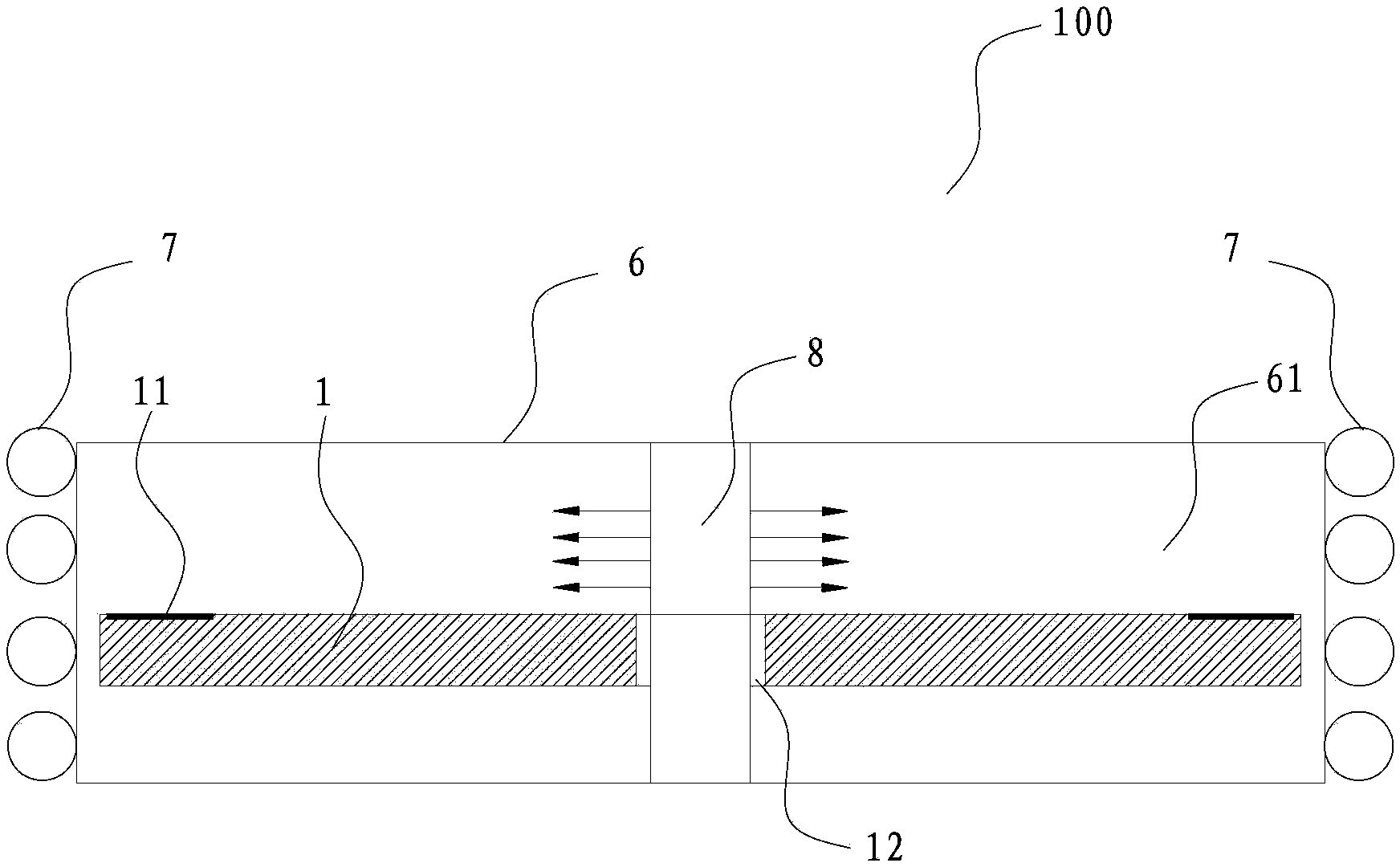
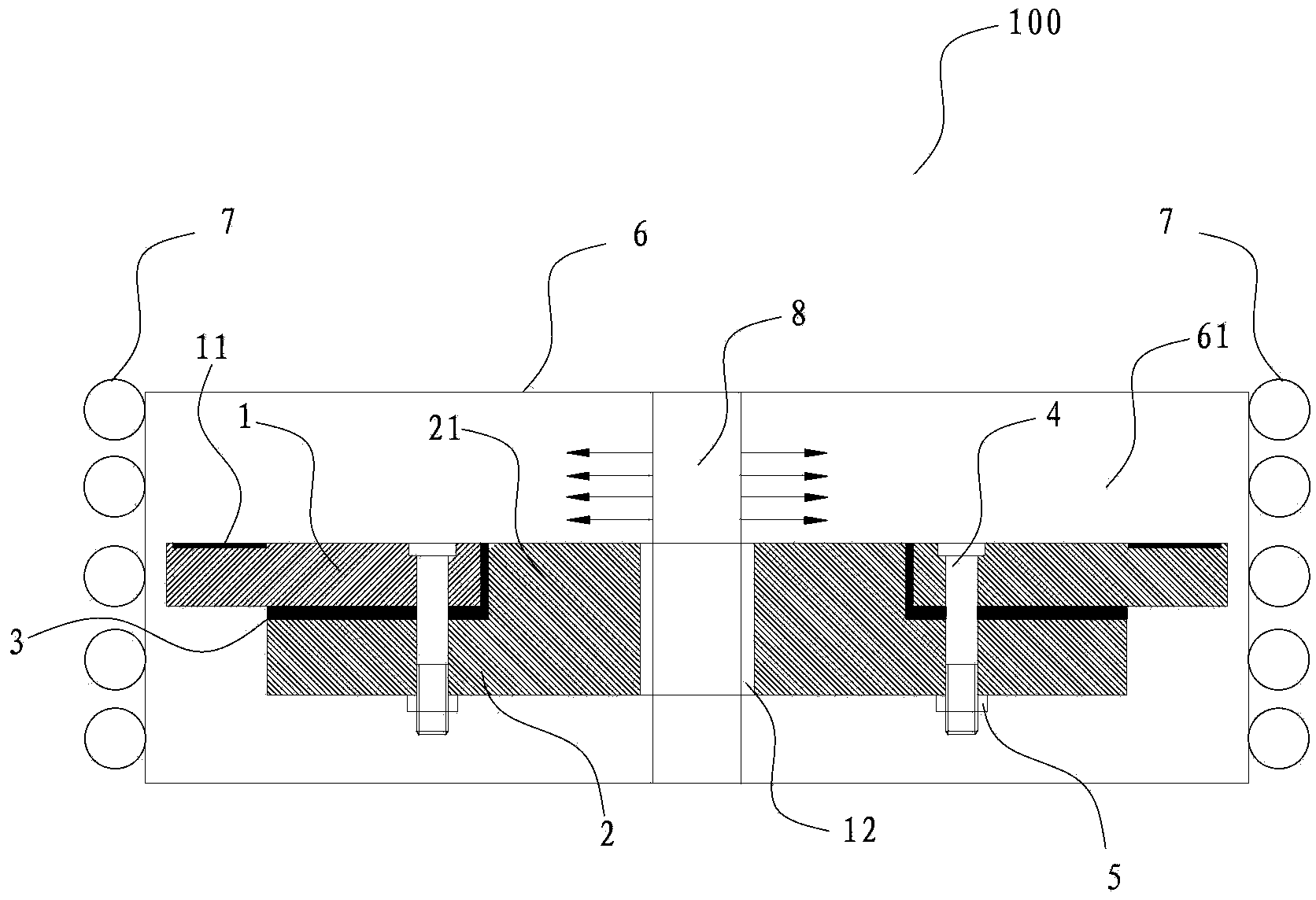
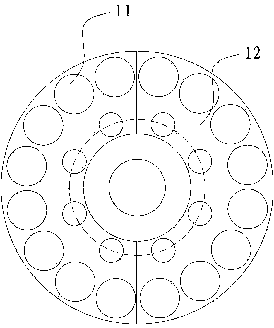
[0034] Embodiments of the present invention are described in detail below, examples of which are shown in the drawings, wherein the same or similar reference numerals designate the same or similar elements or elements having the same or similar functions throughout. The embodiments described below by referring to the figures are exemplary and are intended to explain the present invention and should not be construed as limiting the present invention.

[0035] In describing the present invention, it should be understood that the terms "center", "longitudinal", "transverse", "length", "width", "thickness", "upper", "lower", "front", " Orientation or position indicated by "back", "left", "right", "vertical", "horizontal", "top", "bottom", "inner", "outer", "clockwise", "counterclockwise", etc. The relationship is based on the orientation or positional relationship shown in the drawings, and is only for the convenience of describing the present invention and simplifying the descrip...


PUM


Abstract

The invention discloses semiconductor processing equipment. The semiconductor processing equipment comprises a chamber body having a reaction cavity inside; a first tray arranged inside the reaction cavity and provided with a sheet groove for bearing a wafer; and an inductance coil which surrounds the periphery of the chamber body and is used for heating the first tray, the first tray consisting of a plurality of sub-trays, and physical gaps existing among the sub-trays. According to the semiconductor processing equipment in the invention, the first tray is separated into the plurality of sub-trays, so that influence of a skin effect on the first tray can be effectively reduced, uniformity of temperature distribution of the first tray is improved, and radial gradients of temperature distribution are lowered, thereby enabling a temperature rise of a substrate located inside the sheet groove to be more uniform, and improving a process effect of semiconductor processing equipment.

Description

technical field [0001] The present invention relates to semiconductor processing equipment. Background technique [0002] Semiconductor processing equipment is widely used in the field of semiconductor processing. In the process of semiconductor processing, as the requirements for processing accuracy become higher and higher, the temperature uniformity of the wafer surface has attracted more and more attention, especially in the processing of LED epitaxial wafers. In order to increase productivity, multiple wafers are usually placed on a tray for simultaneous processing. In order to obtain good process consistency, the temperature of multiple wafers placed on the surface of the tray should be kept as consistent as possible, which requires that the temperature distribution on the surface of the tray should be As evenly as possible. Especially metal organic compound chemical vapor deposition (MOCVD) technology in the LED field is a compound semiconductor vapor phase epitaxy t...

Claims


Application Information

Patent Timeline
IPC IPC(8): H01L21/67
CPCH01L21/67333
Inventor 袁福顺
Owner BEIJING NAURA MICROELECTRONICS EQUIP CO LTD
Why Eureka
Try Eureka