Hybrid bonding mechanisms for semiconductor wafers

A hybrid bonding, semiconductor technology, used in semiconductor/solid-state device manufacturing, semiconductor devices, semiconductor/solid-state device components, etc.

Active Publication Date: 2014-05-14
TAIWAN SEMICON MFG CO LTD
View PDF6 Cites 27 Cited by
  • Summary
  • Abstract
  • Description
  • Claims
  • Application Information

AI Technical Summary

Problems solved by technology

However, there are still many challenges associated with 3DIC

Method used


Image

  • Hybrid bonding mechanisms for semiconductor wafers
  • Hybrid bonding mechanisms for semiconductor wafers
  • Hybrid bonding mechanisms for semiconductor wafers

Examples


Embodiment Construction

[0040] The making and using of embodiments of the invention are discussed in detail below. It should be appreciated, however, that the present invention provides many applicable inventive concepts that can be embodied in a wide variety of specific contexts. The specific embodiments discussed are merely illustrative of specific ways to make and use the invention, and do not limit the scope of the invention.

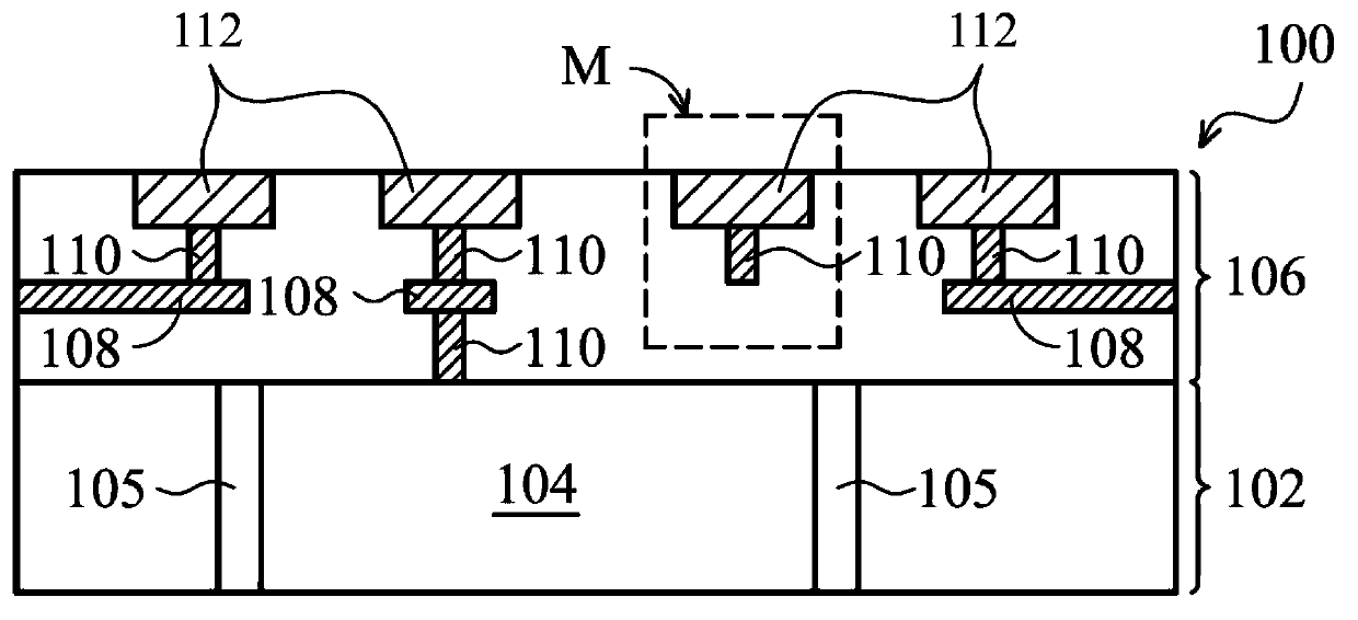
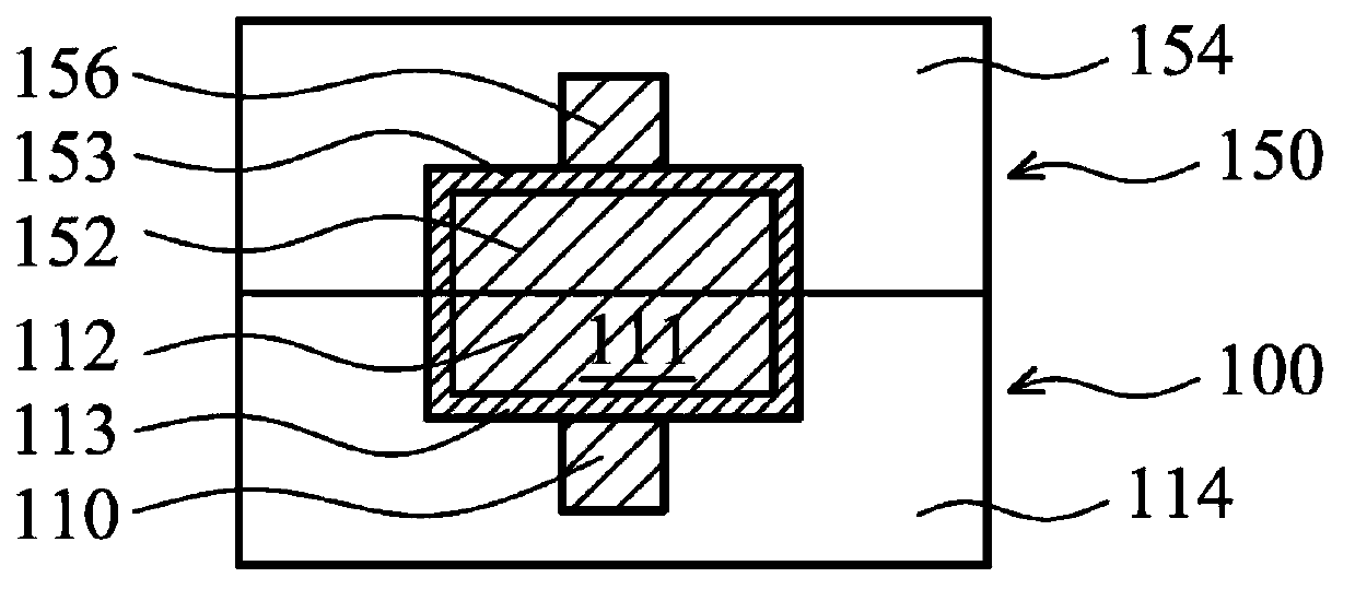
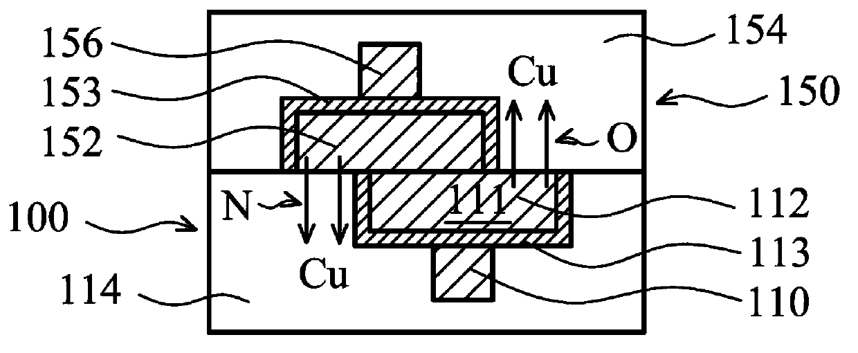
[0041]Hybrid bonding is a type of bonding method used for 3DIC in which two semiconductor wafers are bonded together using a hybrid bonding technique. Some methods and structures for 3DICs formed by hybrid bonding are described in U.S. Serial No. 13 / 488,745, entitled "Three Dimensional Integrated Circuit Structures and Hybrid Bonding Methods for Semiconductor Wafers," filed June 5, 2012 (Attorney Docket No. TSM3012-0241) and filed July 2012. US Serial No. 13 / 542,507, filed on the 5th, entitled "Hybrid Bonding Systems and Methods for Semiconductor Wafers" (Attorney Docket ...


PUM

PropertyMeasurementUnit
thicknessaaaaaaaaaa
thicknessaaaaaaaaaa

Abstract

The embodiments of diffusion barrier layer described above provide mechanisms for forming a copper diffusion barrier layer to prevent device degradation for hybrid bonding of wafers. The diffusion barrier layer(s) encircles the copper-containing conductive pads used for hybrid bonding. The diffusion barrier layer can be on one of the two bonding wafers or on both bonding wafers.

Description

[0001] Cross References to Related Applications [0002] This application is related to the following co-pending and commonly assigned patent application: "Three Dimensional Integrated Circuit Structures and Hybrid Bonding Methods for Semiconductor Wafers," filed June 5, 2012, (Attorney Docket No. TSM3012 -0241) and U.S. Serial No. 13 / 488,745, filed July 5, 2012, entitled "Hybrid Bonding Systems and Methods for Semiconductor Wafers" (Attorney Docket No. TSM3012-0242) U.S. Serial No. 13 / 542,507. The entire contents of the aforementioned patent applications are hereby incorporated by reference. technical field [0003] The present invention relates to semiconductor devices and, in particular, to hybrid bonding mechanisms for semiconductor wafers. Background technique [0004] Semiconductor devices are used in various electronic applications such as personal computers, mobile phones, digital cameras, and other electronic equipment, for example. Semiconductor devices are typi...

Claims


Application Information

Patent Timeline
Patent Type & Authority Applications(China)
IPC IPC(8): H01L23/488H01L21/60
CPCH01L24/80H01L23/53238H01L23/53295H01L21/76831H01L21/76834H01L24/05H01L24/08H01L25/0657H01L25/50H01L2224/0345H01L2224/0346H01L2224/0347H01L2224/0348H01L2224/0361H01L2224/05026H01L2224/05147H01L2224/05187H01L2224/05564H01L2224/05571H01L2224/05578H01L2224/05647H01L2224/05687H01L2224/80121H01L2224/80203H01L2224/05576H01L2224/03616H01L2225/06513H01L2224/08121H01L2924/00014H01L2224/05553H01L2224/05547H01L24/03H01L2224/02126H01L2224/02125H01L2224/8034H01L2224/80895H01L2224/80896H01L2224/08058H01L2224/80357H01L2224/80359H01L2224/08145H01L2924/05442H01L2924/04953H01L2924/00012H01L2924/05042H01L2924/059H01L2924/04941H01L2924/05032H01L2224/05552H01L2224/0508H01L2924/0504H01L2224/08147
Inventor 刘丙寅陈思莹王铨中黄志辉黄信华赵兰璘杜友伦蔡嘉雄陈晓萌
Owner TAIWAN SEMICON MFG CO LTD
Why Eureka
Try Eureka