Non-complementary flyback active clamp converter
A non-complementary, converter technology, applied in the direction of converting DC power input to DC power output, instrumentation, and adjusting electrical variables, etc. It can solve the problems that the clamp switch Sa cannot realize soft switching, large turn-on loss, and cannot release energy. , to achieve the effect of reducing circuit efficiency, reducing high-frequency oscillation, and increasing on-state loss
- Summary
- Abstract
- Description
- Claims
- Application Information
AI Technical Summary
Problems solved by technology
Method used
Image
Examples
Embodiment 1
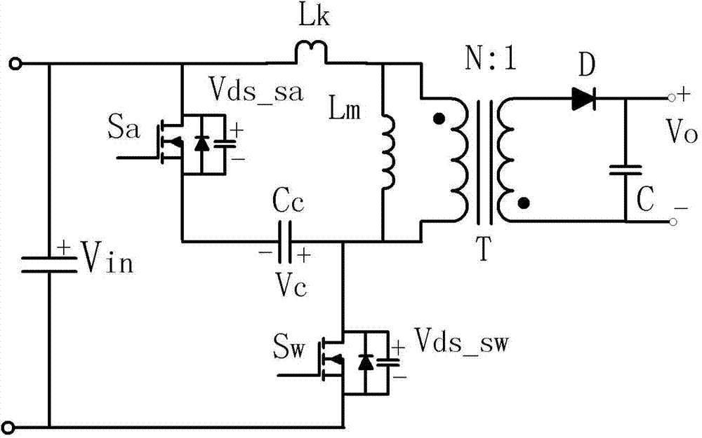
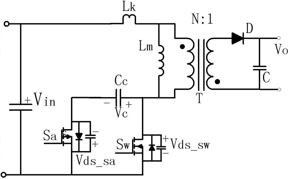
[0046] Such as Figure 7-1 As shown, the non-complementary flyback active clamp converter of Embodiment 1 of the present invention includes a transformer T, a main switch tube Sw, a clamp switch tube Sa, a clamp capacitor Cc, a drive module and an isolated drive circuit. The primary winding and the main switching tube Sw are connected in series for the input voltage signal, the secondary winding of the transformer T is used for outputting the transformed voltage signal, and the clamping switching tube Sa is an NMOS tube, which is connected in series with the clamping capacitor Cc to the transformer The primary windings of T are connected in parallel. The driving module outputs the main driving signal Vgs_sw for controlling the main switching tube Sw to be turned on and off alternately to the driving end of the main switching tube Sw, and the driving module outputs the clamping driving signal Vgs_sa to the driving end of the clamping switching tube Sa, The clamp drive signal V...
Embodiment 2
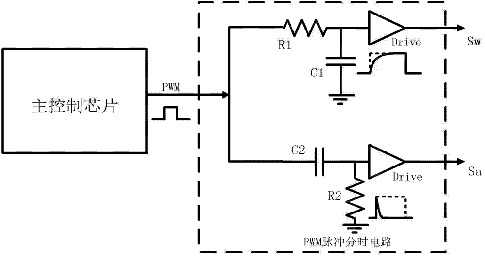
[0062] Such as Figure 9 As shown, the non-complementary flyback active clamp converter of the second embodiment of the present invention is basically the same as the first embodiment, and their difference is that in the second embodiment, the driving module includes a main control circuit and a second control detection circuit, They can be integrated in one chip.
[0063] see Figure 10 The main control circuit of the second embodiment includes a clock oscillator OSC, a second pulse signal module Narrow Pulse2 for forming a second pulse signal Vgs_sa2, a second delay circuit Delay2, a logic circuit Logic, a ramp circuit Slope and a drive circuit Drive, the second control detection circuit includes the third delay circuit Delay3 and the first pulse signal module Narrow Pulse1; the output end of the clock oscillation generator OSC is connected to the input end of the second pulse signal module Narrow Pulse2 one way, and the other way is connected to the first pulse signal modu...
PUM
 Abstract
Description
Claims
Application Information


