A kind of multi-layer circuit board and its impedance control method

A multi-layer circuit board, impedance control technology, applied in the direction of printed circuit components, electrical connection printed components, etc., can solve the problem of lack of impedance control methods

Active Publication Date: 2017-06-27
LENOVO (BEIJING) LTD
View PDF5 Cites 0 Cited by
  • Summary
  • Abstract
  • Description
  • Claims
  • Application Information

AI Technical Summary

Problems solved by technology

[0022] Embodiments of the present invention provide a multi-layer circuit board and its impedance control method to solve the technical problem of lacking a more feasible impedance control method in the prior art

Method used


Image

  • A kind of multi-layer circuit board and its impedance control method
  • A kind of multi-layer circuit board and its impedance control method
  • A kind of multi-layer circuit board and its impedance control method

Examples


Embodiment Construction

[0044] Embodiments of the present invention provide a multilayer circuit board and an impedance control method thereof to solve the technical problem of lacking a more feasible impedance control method in the prior art.

[0045] The technical solution in the embodiments of the present invention is to solve the above-mentioned technical problems, and the general idea is as follows:

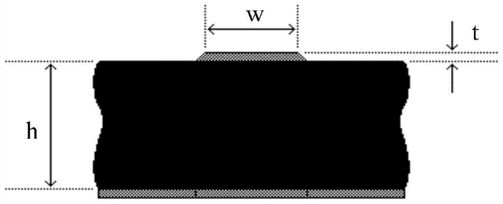
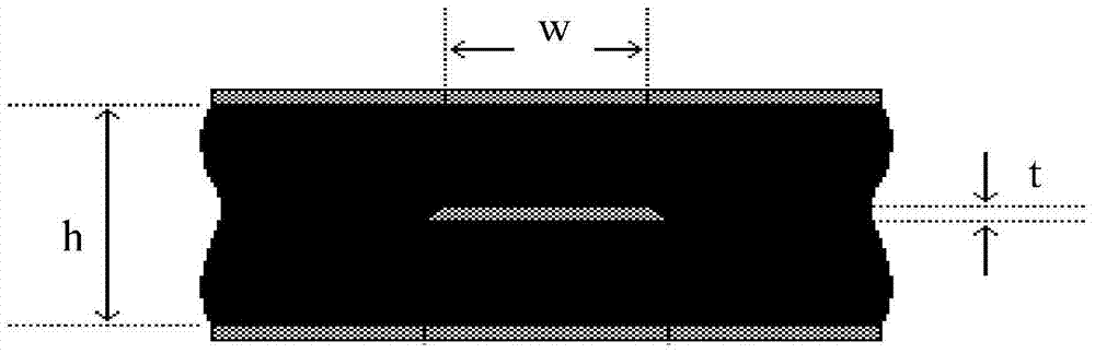
[0046]In an embodiment of the present invention, the multi-layer circuit board includes: a first insulating layer; a first mesh grounding layer arranged on the bottom surface of the first insulating layer, and a plurality of grids are formed on the grounding layer; a transmission line layer including At least one transmission line is formed on the surface of the first insulating layer; a plurality of via holes penetrate the first insulating layer and the first mesh ground layer; the positions of the plurality of via holes overlap with the positions of the grids and / or are located in multiple grids ...


PUM


Abstract

The invention provides a multi-layer circuit board and a method for controlling the impedance of the multi-layer circuit board. The multi-layer circuit board comprises a first insulating layer, a first net-shaped ground layer, a transmission line layer and a plurality of via holes, wherein the first net-shaped ground layer is arranged on the bottom surface of the first insulating layer, a plurality of meshes are formed on the ground layer, the transmission line layer comprises at least one transmission line and is formed on the surface of the first insulating layer, and the via holes penetrate through the first insulating layer and the first net-shaped ground layer. The positions of the multiple via holes and the positions of the meshes overlap and / or the via holes are located at the intersection positions of the multiple meshes.

Description

technical field [0001] The invention relates to the technical field of semiconductor manufacturing, in particular to a multilayer circuit board and an impedance control method thereof. Background technique [0002] The characteristic impedance of the wire on the printed circuit board refers to the resistance that the high-frequency signal or electromagnetic wave receives when the transmission line is transmitted. It refers to the joint resistance of the resistance, inductance and capacitance to the alternating current. Its symbol is Z 0 , referred to as impedance, the unit is ohm (Ω). The characteristic impedance Z of the transmission line 0 In the case of no loss, it can be obtained from the inductance (L) per unit length of the transmission line and the capacitance (C) per unit length. The relationship is: [0003] [0004] Characteristic impedance is an important indicator of circuit board design, especially in the design of PCB (Printed Circuit Board; printed circui...

Claims


Application Information

Patent Timeline
Patent Type & Authority Patents(China)
IPC IPC(8): H05K1/02H05K1/11
Inventor 石彬
Owner LENOVO (BEIJING) LTD
Why Eureka
Try Eureka