
Method for optimizing mutual compensation of surface-shape error of optical system

A surface error and optical system technology, applied in optics, optical components, instruments, etc., can solve the problems of difficult to find the combination of optical components, reduce imaging performance, long assembly time, etc., and achieve significant beneficial effects and efficient assembly , The effect of saving assembly time

Active Publication Date: 2014-05-21
BEIJING INSTITUTE OF TECHNOLOGYGY
View PDF4 Cites 11 Cited by
  • Summary
  • Abstract
  • Description
  • Claims
  • Application Information

AI Technical Summary

Problems solved by technology

Obviously, this manual adjustment method has great chance and randomness, and the assembly time is long and the efficiency is low, especially when the number of lenses is large and contains reflective optical elements, such as catadioptric lithography projection objectives, as many as nearly 30 There are nearly 50 optical surfaces in total, and it is difficult to find the globally optimal combination of optical elements through manual random adjustment, which reduces the imaging performance after system integration

Method used


Image

  • Method for optimizing mutual compensation of surface-shape error of optical system
  • Method for optimizing mutual compensation of surface-shape error of optical system
  • Method for optimizing mutual compensation of surface-shape error of optical system

Examples


Embodiment

[0073] The following takes the designed immersion projection lithography objective lens with a numerical aperture of 1.2 as an example to illustrate the optimization process of the present invention for obtaining the optimal rotation angle combination of all optical elements.

[0074] Such as Figure 4Shown is a designed immersion projection lithography objective lens with a numerical aperture of 1.2 (refer to US Patent US20050190435). The objective lens adopts an off-axis rectangular field of view design. The immersion liquid is deionized water. It consists of 23 lenses and 2 reflectors, with a total of 48 optical surfaces. The maximum system diameter is 278mm, and the total system length is 1217mm. Through design optimization, various design indicators meet the requirements of industrial lithography objective lenses, among which the maximum monochromatic wave aberration root mean square is 5m, and the maximum distortion is 0.5nmn. This catadioptric projection lithography ob...


PUM


Abstract

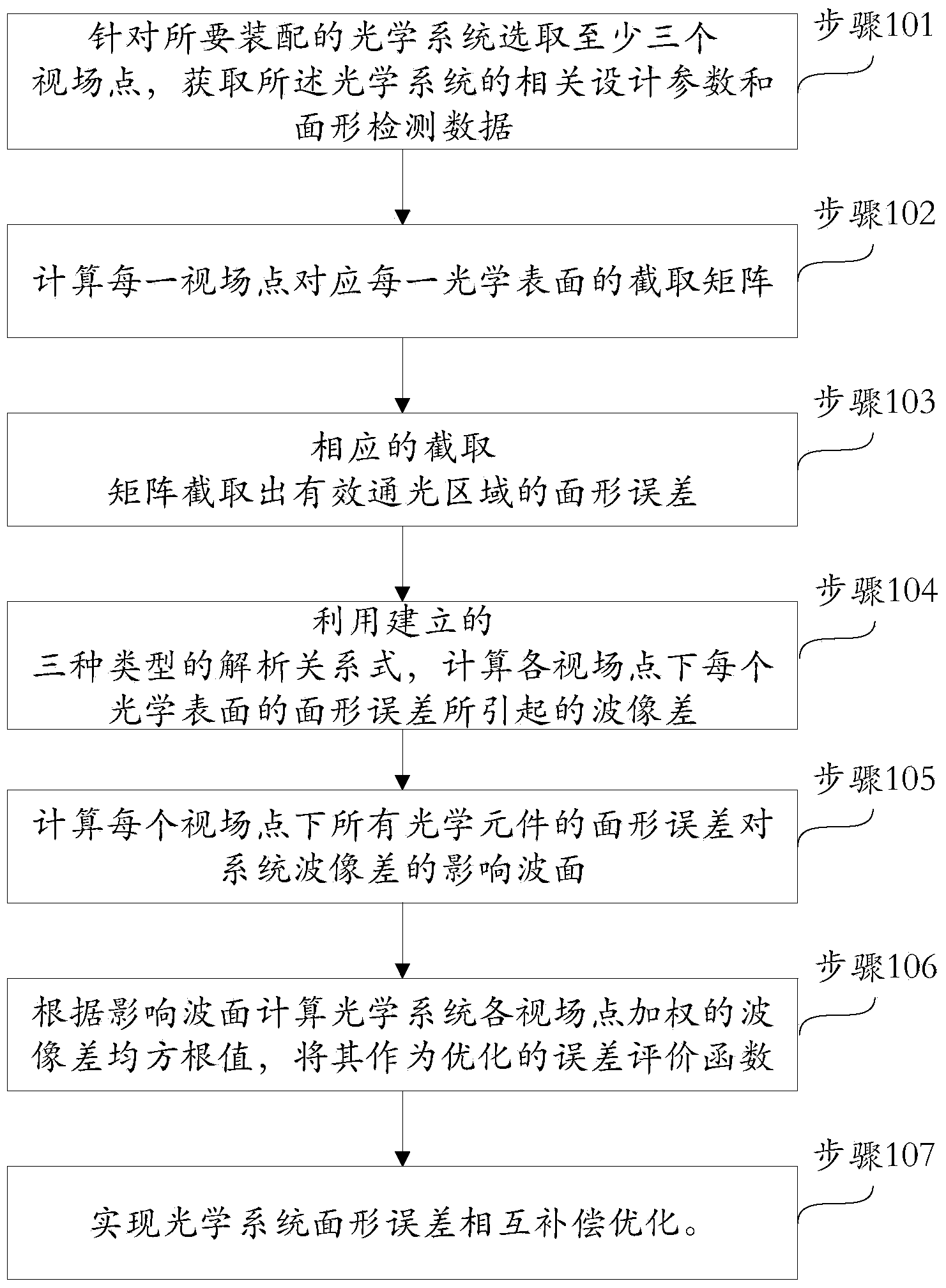
The invention provides a method for optimizing mutual compensation of a surface-shape error of an optical system. The method specifically comprises the steps of firstly, establishing an approximate analysis relation of influence of surface-shape errors of different optical surface types on the wave aberration of the optical system so that the influence of the surface-shape error on the system wave aberration is obtained through directly analysis and calculation independently of an optical structure without light ray tracking calculation by taking the optical structure into account when the rotation angle of an optical element is optimized, secondly, taking the weighted average of the wave aberration,caused by the surface-shape error, of each field-of-view point as an error function of optimization design, and finally, optimizing the rotation angles of all optical elements, and taking the rotation angle, corresponding to that an error evaluation function is minimized, of each optical element as the optimal rotation angle for assembly, and thus realizing mutual compensation optimization of the surface-shape error of the optical system. The assembly efficiency of the optical system is greatly improved by the method.

Description

technical field [0001] The invention relates to an optimization method for mutual compensation of surface shape errors of an optical system, which belongs to the technical field of optimization design of aberration compensation in high-precision optical system processing and assembly. Background technique [0002] Due to the limitation of the optical processing technology level, the surface shape error (low frequency component) of the optical surface is one of the inevitable optical processing errors, which will lead to the deterioration of the imaging performance of the system such as wave aberration, thus far deviating from the image in the system design stage. quality level, especially for high-precision high-performance reflective or catadioptric optical systems. In addition, surface shape errors mainly cause asymmetric aberrations such as astigmatism, which cannot be compared with other optical processing errors such as curvature radius errors, center thickness errors, ...

Claims


Application Information

Patent Timeline
Patent Type & Authority Applications(China)
IPC IPC(8): G02B27/00
Inventor 李艳秋刘晓林
Owner BEIJING INSTITUTE OF TECHNOLOGYGY
Learn More