Ultra high-speed optical analog-to-digital conversion device

An optical mode, ultra-high-speed technology, applied in the field of optical information processing, can solve the problems of application limitation, limited sampling rate, limited number of channels, limited pulse laser source repetition frequency, etc., and achieve high bandwidth, increase sampling rate, and improve sampling rate. Effect

Active Publication Date: 2014-05-21
交芯科(上海)智能科技有限公司
View PDF5 Cites 35 Cited by
  • Summary
  • Abstract
  • Description
  • Claims
  • Application Information

AI Technical Summary

Problems solved by technology

The sampling rate of PADC based on time division multiplexing is limited by the optical switch speed and the accuracy of optical time synchronization required in the demultiplexing process, so its application is limited
The demultiplexing process based on wavelength division multiplexing technology is very simple, but the number of available channels is limited by the bandwidth of optical devices such as the repetition frequency of the pulsed laser source and the available spectral width, which limits the increase in sampling rate.

Method used


Image

  • Ultra high-speed optical analog-to-digital conversion device
  • Ultra high-speed optical analog-to-digital conversion device
  • Ultra high-speed optical analog-to-digital conversion device

Examples


Embodiment Construction

[0027] A specific implementation example of the present invention is given below in conjunction with the accompanying drawings. This embodiment is implemented on the premise of the technical solution of the present invention, and detailed implementation methods and processes are given, but the protection scope of the present invention is not limited to the following embodiments.

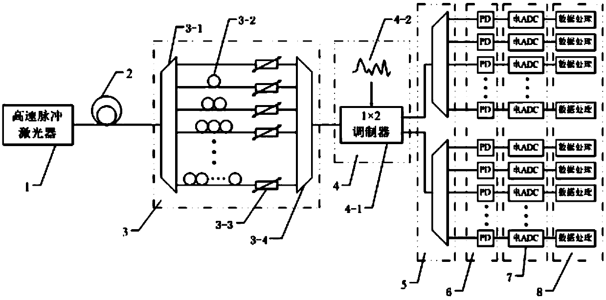
[0028] refer to figure 1 , figure 1 It is a schematic structural diagram of an ultra-high-speed optical analog-to-digital conversion device of the present invention. As shown in the figure, an ultra-high-speed optical analog-to-digital conversion device includes a high-speed pulse laser 1, a spectrum broadening module 2, and a repetition rate multiplication module 3 connected in sequence. Ultra-wideband signal sampling module 4 , wavelength multi-channelization module 5 , parallel photoelectric conversion module 6 , parallel electrical quantization module 7 and parallel data processing module 8 .

...


PUM


Abstract

The invention relates to an ultra high-speed optical analog-to-digital conversion device. The ultra high-speed optical analog-to-digital conversion device comprises a high-speed pulse laser, a frequency spectrum broadening module, a repetition frequency multiplication module, an ultra wide band signal sampling module, a wavelength multi-channelizing module, parallel photoelectric conversion modules, parallel electric quantization modules and parallel data processing modules, wherein the high-speed pulse laser, the frequency spectrum broadening module, the repetition frequency multiplication module, the ultra wide band signal sampling module, the wavelength multi-channelizing module, the parallel photoelectric conversion modules, the parallel electric quantization modules and the parallel data tprocessing modules are sequentially connected. According to the ultra high-speed optical analog-to-digital conversion device, the high-speed pulse laser and the wavelength-division multiplexing technology are combined, while the advantages that the wavelength-division multiplexing technology is simple and practicable are kept, the defect that the output frequency spectrum of an active mode-locking fiber laser is narrow is overcome through the frequency spectrum broadening technology, high-speed photoelectric sampling is carried out through a broadband 1*2 electro-optical modulator, and by increasing the number of wavelength-division multiplexing channels or the number of parallel channels of the system, the bandwidth of a photoelectric detector and the sampling rate of an electric analog-to-digital converter are not increased while the sampling rate of the system is improved.

Description

technical field [0001] The invention relates to the technical field of optical information processing, in particular to an ultra-high-speed optical analog-to-digital conversion device. Background technique [0002] Signals in nature exist in continuous form, that is, analog signals. In order to facilitate signal transmission, processing and storage, analog signals need to be converted into digital signals. Therefore, the analog-to-digital converter is a bridge connecting the analog world and the digital world. In recent years, electrical analog-to-digital conversion (EADC) technology has developed rapidly. The highest sampling rate of commercial chips in the world is about 30Gs / s, 5.5bit, and the analog bandwidth that the corresponding equipment can handle can reach 30GHz. However, these indicators are close to the theoretical limit of electricity, and further improvement faces great challenges. This is because the design, manufacture and packaging of EADC are all based on t...

Claims


Application Information

Patent Timeline
Patent Type & Authority Applications(China)
IPC IPC(8): G02F7/00
Inventor 邹卫文李杏张华杰吴龟灵陈建平
Owner 交芯科(上海)智能科技有限公司
Why Eureka
Try Eureka