Semiconductor light-emitting chip, semiconductor lighting fixture and manufacturing method thereof

A technology of light-emitting chips and semiconductors, which is applied in the direction of semiconductor devices, semiconductor devices of light-emitting elements, lighting devices, etc., can solve the problems of high comprehensive manufacturing costs of lamps, increased process links and production equipment, and accelerated light decay of light-emitting chips. Achieve no heat conduction bottleneck, save the use of raw materials, and improve the effect of heat dissipation

Active Publication Date: 2016-11-09
SHENZHEN DADAO SEMICON CO LTD
View PDF9 Cites 0 Cited by
  • Summary
  • Abstract
  • Description
  • Claims
  • Application Information

AI Technical Summary

Problems solved by technology

Repeating the fixation three times not only wastes a lot of raw materials and increases the weight of the lamp, but also adds many insignificant process links and production equipment, which makes the comprehensive manufacturing cost of the lamp high.
Poor heat dissipation will cause the light-emitting chip 380 to decay faster and shorten the service life of the whole lamp

Method used


Image

  • Semiconductor light-emitting chip, semiconductor lighting fixture and manufacturing method thereof
  • Semiconductor light-emitting chip, semiconductor lighting fixture and manufacturing method thereof
  • Semiconductor light-emitting chip, semiconductor lighting fixture and manufacturing method thereof

Examples


Embodiment Construction

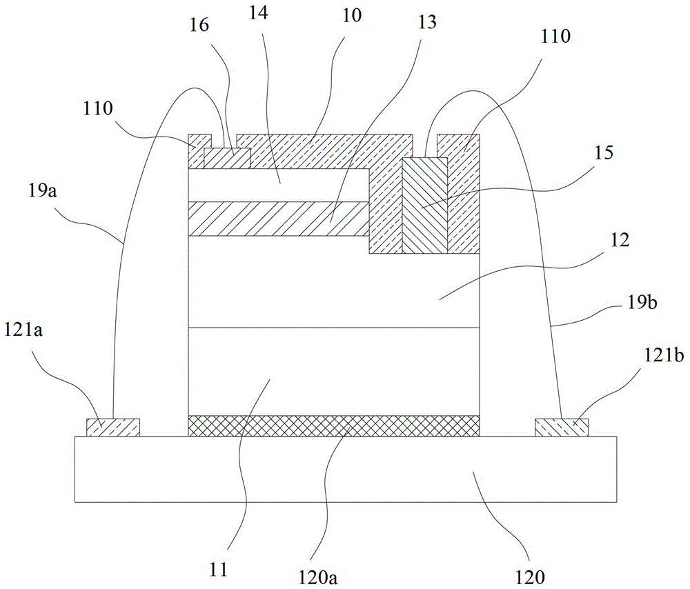
[0055] Such as Figure 4 Shown is an embodiment of a semiconductor light-emitting chip suitable for reflow soldering in the present invention, including a sapphire substrate 41, an n-type conductive layer 42, a light-emitting layer 43, a p-type conductive layer 44, an n-type electrode 45, a p-type Electrodes 46, n-type pads 45a, p-type pads 46a, metal-based thermal pads 47a, insulating layers 410, 410a, current spreading layers 44b, n-type electrode steps 44a, sapphire substrate steps 44c, LED brackets 420, n Type pad 420a, p-type pad 420b, thermal pad 420c, metal solder 421a, 421b, 421c, etc. Among them, the n-type conductive layer, the light-emitting layer and the p-type conductive layer together form a semiconductor stack; the sapphire substrate 41, the n-type conductive layer 42, the light-emitting layer 43, the p-type conductive layer 44, the n-type electrode 45, the p-type electrode 46. ​​N-type welding pad 45a, p-type welding pad 46a, metal-based heat-conducting pad 47...


PUM


Abstract

The invention relates to a semiconductor light-emitting chip and a lamp using the chip. The chip includes a substrate having a first surface and a second surface, on the first surface of the substrate there is a semiconductor stack including at least an n-type conductive layer, a light-emitting layer and a p-type conductive layer, and on the semiconductor stack The surface has at least one n-type electrode step and / or n-type electrode through hole exposing a part of the n-type conductive layer, and all exposed and conductive surfaces and sides of the semiconductor light emitting chip are wrapped by at least one insulating layer; The surface of the insulating layer is provided with exposed at least one p-type electrode and at least one n-type electrode; the p-type electrode and the n-type electrode are insulated from each other, and penetrate through the insulating layer and the p-type conductive layer and the n-type electrode respectively. The conductive layer is electrically connected. Its structure allows the semiconductor light-emitting chip to be directly welded to the lamp board, lamp bar, lamp post, or LED bracket, or COB substrate used to prepare various lamps or light sources by reflow soldering process, which has the advantages of simple structure and low manufacturing cost .

Description

technical field [0001] The present invention relates to a semiconductor light emitting chip, and further relates to a semiconductor light emitting chip structure suitable for reflow soldering. Background technique [0002] With the improvement of luminous efficiency and the reduction of manufacturing cost of semiconductor light-emitting chips, semiconductor light-emitting chips have been widely used in fields such as backlight, display and lighting. [0003] A common semiconductor light-emitting chip structure such as figure 1 As shown, it includes a sapphire substrate 11, an n-type conductive layer 12, a light-emitting layer 13, a p-type conductive layer 14, an n-type electrode 15, a p-type electrode 16, conductive lines 19a, 19b, an insulating layer 110, pads 121a, 121b , LED bracket 120, crystal bonding adhesive 120a. In order to reduce the shading effect and increase the effective light-emitting area, the size of the electrodes 15 and 16 is reduced as much as possible,...

Claims


Application Information

Patent Timeline
Patent Type & Authority Patents(China)
IPC IPC(8): H01L33/48H01L33/62F21V29/503F21Y115/10F21V29/71F21V29/89
CPCH01L33/38H01L33/62H01L33/647F21V29/00F21Y2101/00H01L2933/0066H01L2224/0401H01L2224/04042H01L2224/0603H01L2224/06102H01L2224/1703H01L2224/49
Inventor 李刚
Owner SHENZHEN DADAO SEMICON CO LTD
Why Eureka
Try Eureka