Single-mode photonic crystal edge-emitting semiconductor laser device

A technology of photonic crystals and semiconductors, which is applied to the structure of semiconductor lasers, lasers, and optical waveguide semiconductors. It can solve problems such as large changes, intensified side-mode competition, and increased far-field angles, and achieves low cost, compact structure, and ease of use. integrated effect

Active Publication Date: 2014-05-28
INST OF SEMICONDUCTORS - CHINESE ACAD OF SCI
View PDF5 Cites 10 Cited by
  • Summary
  • Abstract
  • Description
  • Claims
  • Application Information

AI Technical Summary

Problems solved by technology

To obtain high power, a wide waveguide structure must be used, and a wide waveguide will inevitably generate multiple side modes, which will intensify the competition of the side modes, increase the far field angle, and change greatly with the current

Method used


Image

  • Single-mode photonic crystal edge-emitting semiconductor laser device
  • Single-mode photonic crystal edge-emitting semiconductor laser device
  • Single-mode photonic crystal edge-emitting semiconductor laser device

Examples


Embodiment

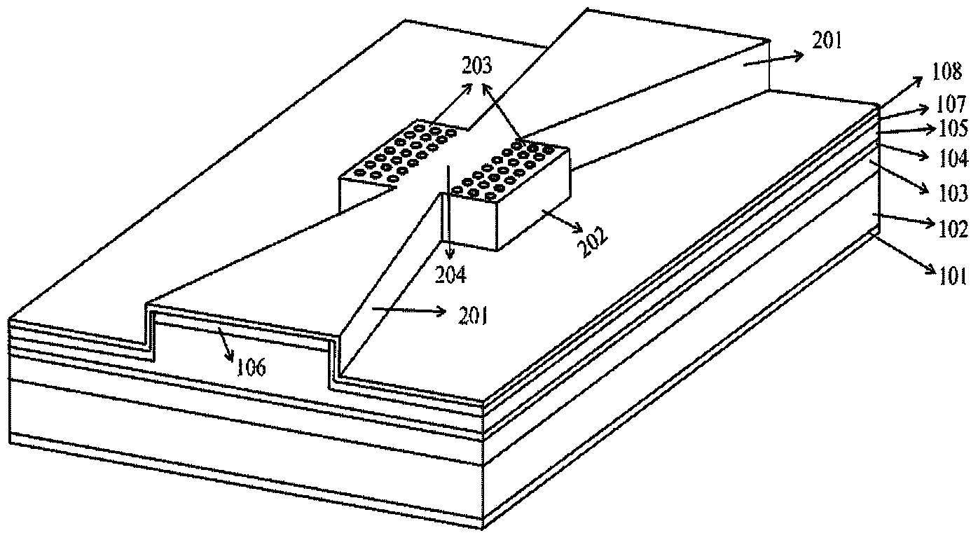
[0038] figure 1 It is a three-dimensional structural schematic diagram of an embodiment of a single-mode photonic crystal edge-emitting semiconductor laser. The lasing wavelength of the semiconductor laser is 913 nm, and the total length of the device is 1300 μm. Among them, the length of the mode selection region is 300 μm, and the length of the two symmetrically distributed mode amplification regions is 500 μm. In the mode selection area, the width of the air hole arrays 203 on the left and right sides of the photonic crystal waveguide 202 is 27.5 μm, the period and duty cycle are 3.05 μm and 0.5 respectively, and the width of the line defect 204 is 5 μm. In the mode amplification region, the width of a single tapered waveguide 201 increases linearly from 5 μm at the narrow port to 60 μm at the wide port. The etching depth of the raised three-section waveguide in the middle of the P-type confinement layer 105 and the air hole array 203 is 1.1 μm.

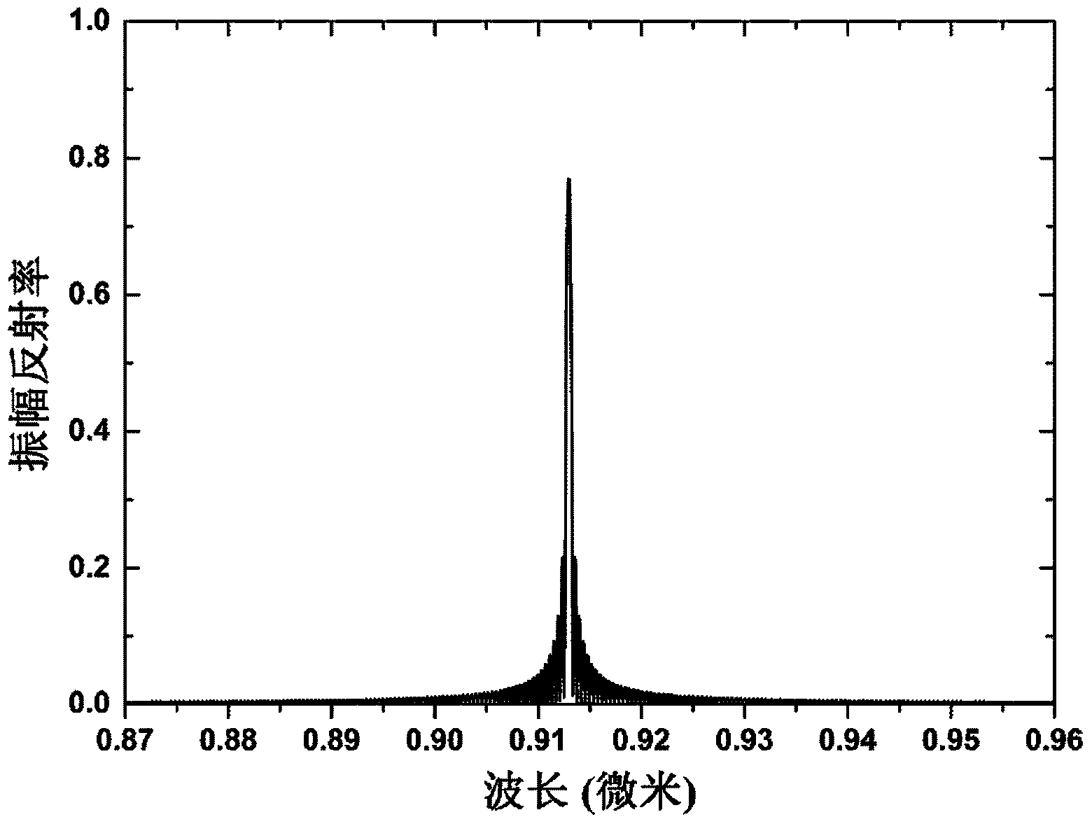
[0039] figure 2 is th...


PUM


Abstract

The invention relates to a single-mode photonic crystal edge-emitting semiconductor laser device. The single-mode photonic crystal edge-emitting semiconductor laser device comprises a laminated structure, wherein the laminated structure comprises a lower electrode, an N-type substrate, an N-type restriction layer, an active layer, a P-type restriction layer, a P-type cover layer, an SiO2 insulated layer and an upper electrode; the N-type substrate is manufactured on the lower electrode; the N-type restriction layer is manufactured on the N-type substrate; the active layer is manufactured on the N-type restriction layer; a three-section type waveguide raised along the longitudinal direction is arranged in the middle of the P-type restriction layer, opposite tapered waveguides are arranged on the two sides of the three-section type waveguide, and a photonic crystal waveguide is arranged between the opposite tapered waveguides and is manufactured on the active layer; the P-type cover layer is manufactured above the three-section type waveguide on the P-type restriction layer; the SiO2 insulated layer is manufactured on the side wall of the three-section type waveguide on the P-type restriction layer and covers upper part of the P-type restriction layer to form a substrate; the upper electrode is manufactured above the substrate except the side wall. Longitudinal mode and side mode of the laser device are selected through the photonic crystal waveguide, and the laser power is amplified by utilizing a symmetrical biconical structure, so that the purpose of high-power, single-mode and low-level divergence angle laser output is achieved.

Description

technical field [0001] The invention relates to the technical field of semiconductor optoelectronic devices, in particular to a single-mode photonic crystal edge-emitting semiconductor laser. Background technique [0002] Semiconductor lasers have high electro-optic conversion efficiency and have the advantages of wide coverage, long life, direct modulation, small size, and low cost. Among them, the edge-emitting semiconductor laser array has great advantages in high-efficiency and high-power laser output. The continuous output power of a single laser bar at room temperature has exceeded 100 watts, and the output power of laser stacks has also exceeded kilowatts. But it also has some problems, the main two of which are poor spectral characteristics and poor far-field performance in the horizontal (parallel to the pn junction plane) direction. The poor spectrum is mainly manifested in the coexistence of multiple longitudinal modes in the cavity, the fierce mode competition, ...

Claims


Application Information

Patent Timeline
Patent Type & Authority Applications(China)
IPC IPC(8): H01S5/065H01S5/20
Inventor 郑婉华刘磊刘云渠红伟张冶金郭文华石岩
Owner INST OF SEMICONDUCTORS - CHINESE ACAD OF SCI
Why Eureka
Try Eureka